Thin film photovoltaic module having a lamination layer for enhanced reflection and photovoltaic output
- Summary
- Abstract
- Description
- Claims
- Application Information
AI Technical Summary
Benefits of technology
Problems solved by technology
Method used
Image
Examples
Embodiment Construction
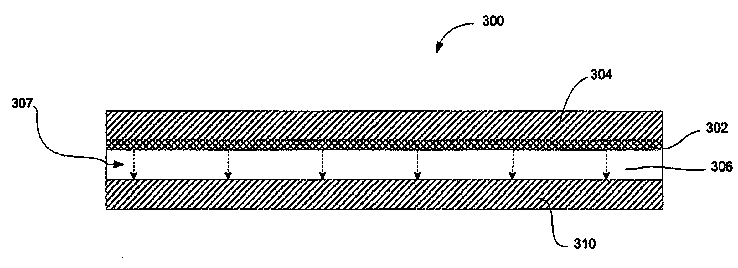
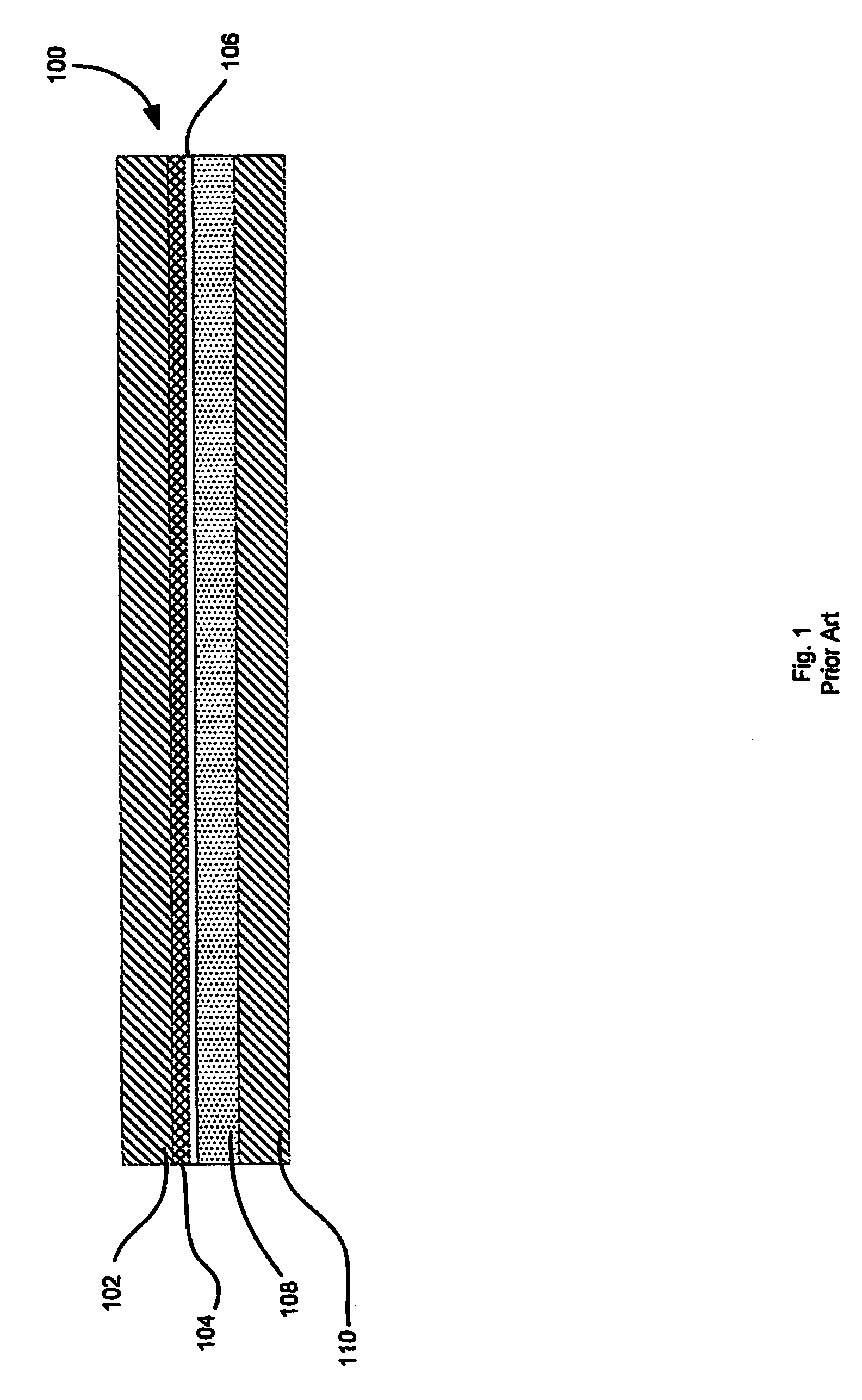
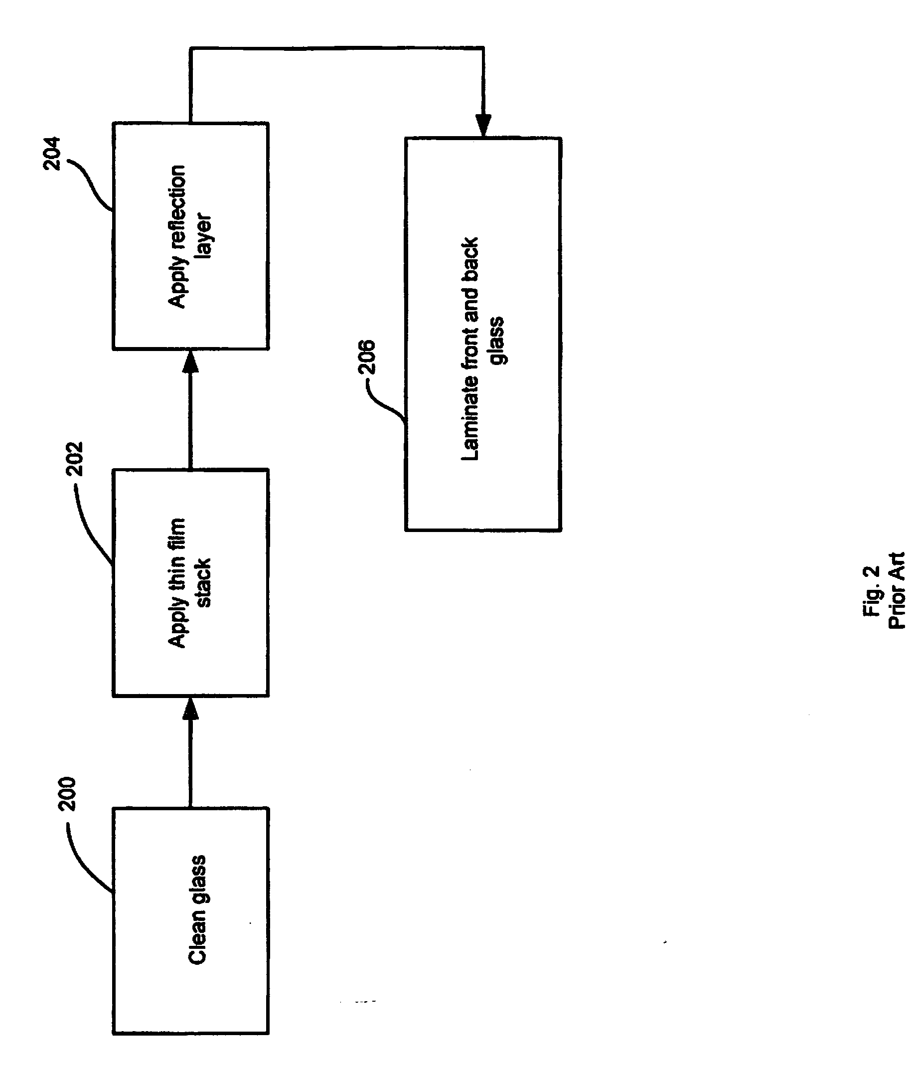
[0025]Referring to the drawings, FIGS. 1 and 2 show a cross section of a conventional thin film PV module 100 and a standard process for making the PV module, respectively. The thin film PV module comprises a transparent substrate 102 such as glass. A light absorbing thin film stack 104 is provided on the interior side of transparent substrate 102 using multiple semiconductor processing steps. An example of a conventional process for forming a light absorbing thin film stack is shown in Schicht et al., U.S. Pat. No. 6,159,621 incorporated herein by reference. The thin film stack 104 can be formed by any well known thin-film PV technology including epitaxial Si, copper indium gallium deselenide (CIGS), cadmium telluride (CdTe), or the like.
[0026]Referring to FIG. 1 and the process in FIG. 2, transparent substrate 102 typically comprises a transparent substrate such as glass that is carefully cleaned as shown at 202 prior to the application of the light-absorbing thin film stack 104. ...
PUM
 Abstract
Description
Claims
Application Information
 - R&D
- Intellectual Property
- Life Sciences
- Materials
- Tech Scout
- Unparalleled Data Quality
- Higher Quality Content
- 60% Fewer Hallucinations
Browse by: Latest US Patents, China's latest patents, Technical Efficacy Thesaurus, Application Domain, Technology Topic, Popular Technical Reports.
© 2025 PatSnap. All rights reserved.Legal|Privacy policy|Modern Slavery Act Transparency Statement|Sitemap|About US| Contact US: help@patsnap.com


