Time to digital converter

a time-to-digital converter and converter technology, applied in the field of time-to-digital converter, can solve the problems of excessively bothersome adjustment work of delay time of tdc performed to acquire periodic data for each dco in use, unnecessarily increasing power consumption, and dulling of waveform

Inactive Publication Date: 2010-11-25
KK TOSHIBA
View PDF2 Cites 25 Cited by
  • Summary
  • Abstract
  • Description
  • Claims
  • Application Information

AI Technical Summary

Benefits of technology

[0011]According to one aspect of the present invention, a time to digital converter includes a delay circuit having a plurality of delay stages that delay an input clock signal in multiple stages, at least one of the delay stages being a variable delay stage; a plurality of flip flops that are provided in a number same as a number of the delay stages of the delay circuit and capture outputs of the delay stages corresponding thereto in parallel in response to input of a reference signal; an edge detecting circuit that detects one or both of rising edges and falling edges of respective outputs of the flip flops; a counter circuit that counts a number of edges detected by the edge detecting circuit; and a control circuit that controls a delay amount of the variable delay stage according to the number of edges counted by the counter circuit.
[0012]According to one aspect of the present inventio

Problems solved by technology

However, the technology of the ADPLL proposed in the past does not indicate a clear guideline concerning a method of deciding the number of delay stages and delay time necessary for obtaining periodic data.
Therefore, adjustment work for delay time of the TDC performed to acquire periodic data for each of DCOs in use is extremely bothersome.
Then, power consumption unnecessarily increases.
On the other hand, to prevent the

Method used


Image

  • Time to digital converter
  • Time to digital converter
  • Time to digital converter

Examples


first embodiment

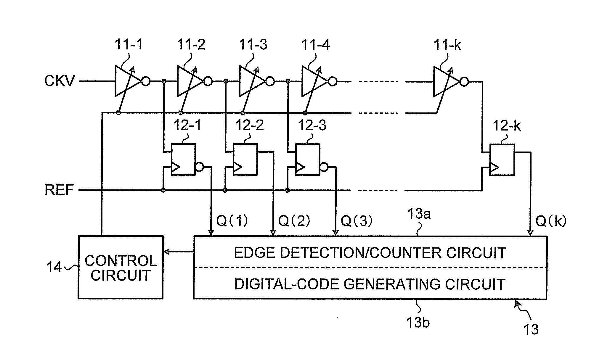
[0031]FIG. 2 is a block diagram illustrating the configuration of a time to digital converter (TDC) according the present invention. In FIG. 2, a TDC according to this embodiment includes a plurality of variable delay circuits 11-1 to 11-k connected in series, a plurality of flip flops 12-1 to 12-k provided in a one-to-one relation with the variable delay circuits 11-1 to 11-k, an edge detection / counter circuit 13a, and a control circuit 14.

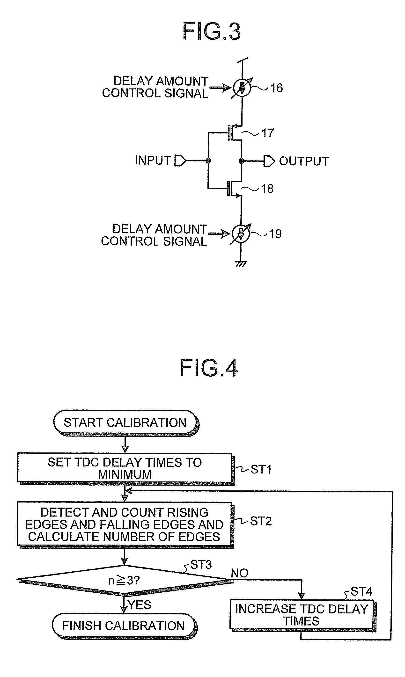
[0032]As the variable delay circuits 11-1 to 11-k, because a delay amount only has to be variable, widely-known variable delay circuits only have to be selected and used as appropriate. Because the variable delay circuits 11-1 to 11-k are shown in FIG. 2 as inverter circuits, a configuration example formed by a CMOS inverter circuit is shown in FIG. 3.

[0033]FIG. 3 is a circuit diagram illustrating a configuration example of the variable delay circuit shown in FIG. 2. In FIG. 3, in a PMOS transistor 17 and an NMOS transistor 18 connected in series...

second embodiment

[0043]FIG. 4 is a flowchart for explaining delay amount control operation of a time to digital converter according to the present invention. FIG. 5 is a timing chart for explaining an optimization process for delay time by a procedure shown in FIG. 4. In FIG. 5, a phase relation between the reference signal REF and the output CKV of the DCO 1, a relation between the output CKV of the DCO 1 and outputs of flip flops at certain delay time, and edge detecting operation are shown.

[0044]In the second embodiment, the edge detection / counter circuit13a shown in FIG. 2 is set to detect and count, at the time of calibration, rising edges and falling edges of output signals of the flip flops 12-1 to 12-k. The control circuit 14 shown in FIG. 2 is set to monitor, at the time of calibration, the number of detected edges n to be three.

[0045]The reference signal REF and the output CKV of the DCO 1 shown in FIG. 2 are input, for example, in a phase relation shown in (1) of FIG. 5 and (2), (3), and ...

third embodiment

[0051]FIG. 6 is a flowchart for explaining delay amount control operation of a time to digital converter according to the present invention. FIG. 7 is a timing chart for explaining an optimization process for delay time by a procedure shown in FIG. 6. In FIG. 7, as in FIG. 5, a phase relation between the reference signal REF and the output CKV of the DCO 1, a relation between the output CKV of the DCO 1 and outputs of flip flops at certain delay time, and edge detecting operation are shown.

[0052]In the third embodiment, the edge detection / counter circuit 13a shown in FIG. 2 is set to detect and count, at the time of calibration, one of rising edges and falling edges of output signals of the flip flops 12-1 to 12-k. In FIGS. 6 and 7, the edge detection / counter circuit 13a is set to detect and count the rising edges. The control circuit 14 shown in FIG. 2 is set to monitor, at the time of calibration, the number of detected edges n to be two.

[0053]The reference signal REF and the outp...


PUM


Abstract

A time to digital converter includes: a delay circuit having a plurality of delay stages that delay an input clock signal in multiple stages, at least one of the delay stages being a variable delay stage; a plurality of flip flops that capture outputs of the delay stages corresponding thereto in a one-to-one relation in response to input of a reference signal; an edge detecting circuit that detects changing edges of respective outputs of the flip flops; a counter circuit that counts a number of edges detected by the edge detecting circuit; and a control circuit that controls a delay amount of the variable delay stage according to the number of edges counted by the counter circuit.

Description

CROSS-REFERENCE TO RELATED APPLICATIONS[0001]This application is based upon and claims the benefit of priority from the prior Japanese Patent Application No. 2009-123327, filed on May 21, 2009; the entire contents of which are incorporated herein by reference.BACKGROUND OF THE INVENTION[0002]1. Field of the Invention[0003]The present invention relates to a time to digital converter.[0004]2. Description of the Related Art[0005]A time to digital converter (hereinafter, “TDC”) is a device that performs measurement of decimal fraction time. In recent years, TDCs having accuracy of nano-second order to pico-second order can be easily realized by a CMOS circuit technology. An application range of the TDCs is extended to various fields. As one of applications of the TDCs, for example, as described in R. B. Staszewski and P. T. Balasare, “All-Digital Frequency Synthesizer in Deep-Submicron CMOS”, Wiley, New York, 2006, an all digital PLL (ADPLL) that is fully digitized by incorporating a TD...

Claims


Application Information

Patent Timeline
IPC IPC(8): H03H11/26H03K5/131H03K5/14H03K5/26H03L7/06
CPCG04F10/005H03L7/07H03L2207/50H03L7/085H03L7/0812
Inventor YOSHIHARA, YOSHIAKIKOBAYASHI, HIROYUKI
Owner KK TOSHIBA
Why Eureka
Try Eureka