Spin transistor and method of operating the same

a technology of spin transistor and spin motor, which is applied in the direction of pulse generator, pulse technique, magnetic body, etc., can solve the problems of increasing the power requirement may not be reduced, and the rate of carrier mobility may not keep

Active Publication Date: 2010-10-28
SAMSUNG ELECTRONICS CO LTD
View PDF21 Cites 12 Cited by
  • Summary
  • Abstract
  • Description
  • Claims
  • Application Information

AI Technical Summary

Benefits of technology

[0073]As described above, spin-polarized electrons may selectively pass through the channel 120 due to the gate voltage, and thus, the spin transistor 100 is turned on. The spin transistor 100 according to example embodiments may have increased charge mobility as compared to a conventional semiconductor device. Also, since the power needed to move spin electrons may be smaller than the power needed to move electrons, the amount of power needed to the operation may be reduced. Accordingly, a relatively small transistor may be manufactured through a scale down.

Problems solved by technology

When semiconductor devices are manufactured to a nanoscale, the increasing rate of carrier mobility may not keep pace with the increasing rate of the semiconductor devices, and despite the reduction in the size of devices, the power requirement may not be reduced.

Method used


Image

  • Spin transistor and method of operating the same
  • Spin transistor and method of operating the same
  • Spin transistor and method of operating the same

Examples


Embodiment Construction

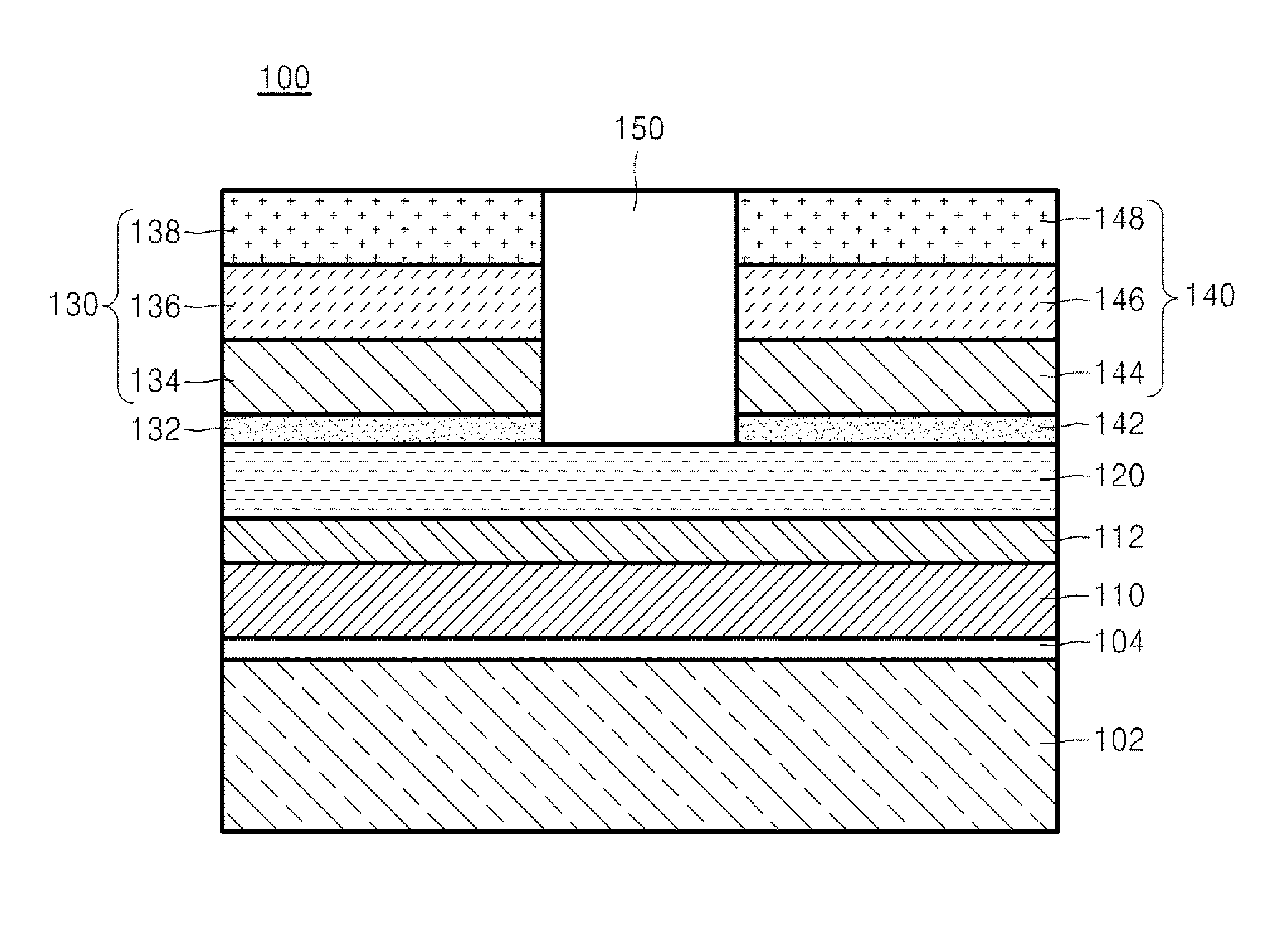
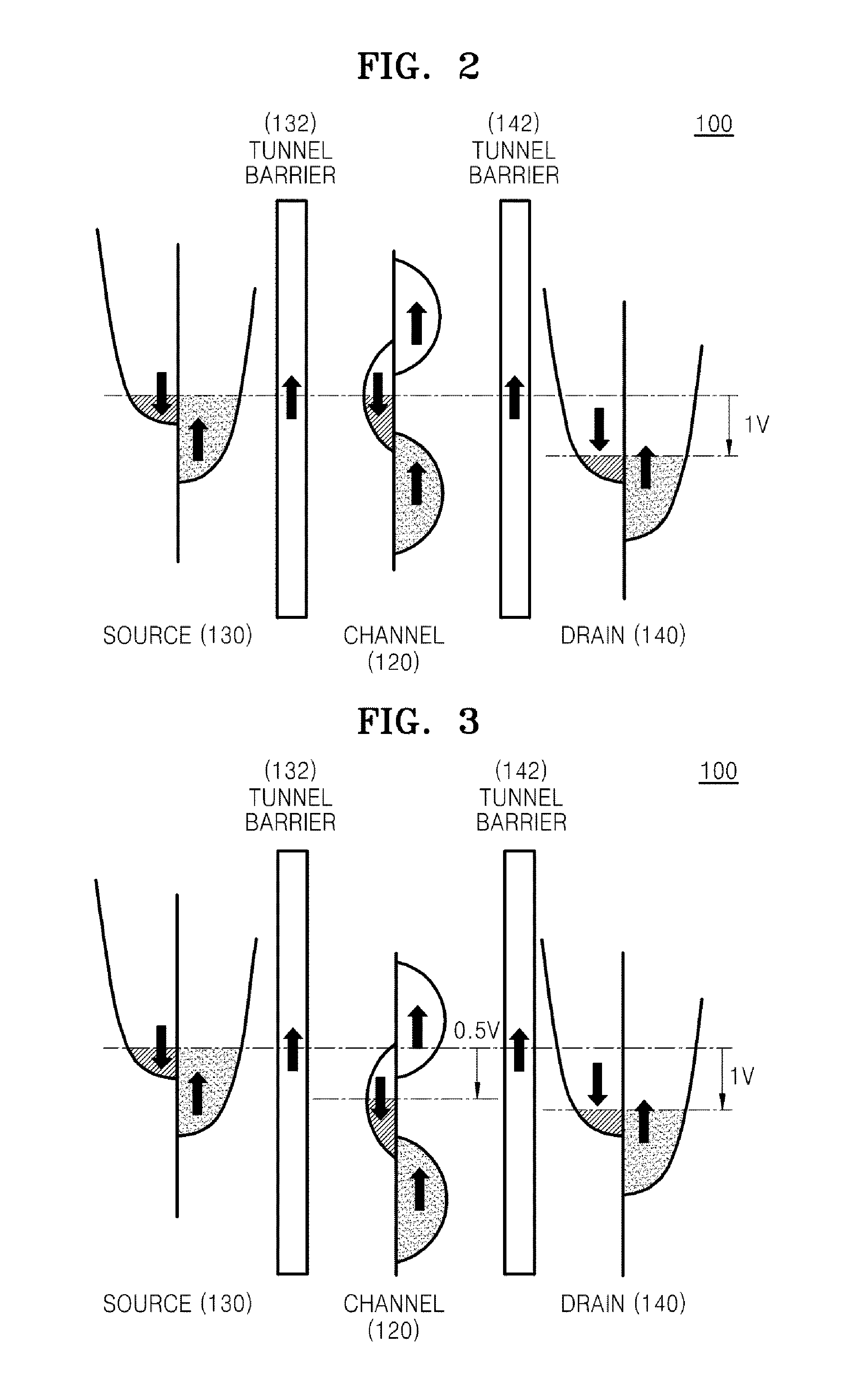
[0042]Example embodiments will now be described more fully with reference to the accompanying drawings in which example embodiments may be shown. In the drawings, the thicknesses of layers and regions may be exaggerated for clarity. Like reference numerals denote like elements in the drawings and repetitive description thereof will be omitted.

[0043]It will be understood that when an element is referred to as being “connected” or “coupled” to another element, it can be directly connected or coupled to the other element or intervening elements may be present. In contrast, when an element is referred to as being “directly connected” or “directly coupled” to another element, there are no intervening elements present. Like numbers indicate like elements throughout. As used herein the term “and / or” includes any and all combinations of one or more of the associated listed items.

[0044]It will be understood that, although the terms “first”, “second”, etc. may be used herein to describe vario...


PUM


Abstract

Disclosed are a spin transistor and a method of operating the spin transistor. The disclosed spin transistor includes a channel formed of a magnetic material selectively passing a spin-polarized electron having a specific direction, a source formed of a magnetic material, a drain, and a gate electrode. When a predetermined voltage is applied to the gate electrode, the channel selectively passes a spin-polarized electron having a specific direction and thus, the spin transistor is selectively turned on.

Description

PRIORITY STATEMENT[0001]This application claims priority under U.S.C. §119 to Korean Patent Application Nos. 10-2007-0114192 and 10-2008-0096725, filed on Nov. 9, 2007, and on Oct. 1, 2008, in the Korean Intellectual Property Office (KIPO), the entire contents of which are incorporated herein by reference.BACKGROUND[0002]1. Field[0003]Example embodiments relate to a spin transistor that uses a field effect and a magnetic field effect.[0004]2. Description of the Related Art[0005]When semiconductor devices are manufactured to a nanoscale, the increasing rate of carrier mobility may not keep pace with the increasing rate of the semiconductor devices, and despite the reduction in the size of devices, the power requirement may not be reduced. In order to address these problems, a technique of using electron spin has been proposed.[0006]As such, a spin transistor is turned on due to the movement of spin-polarized electrons, and the power required to move electrons is small and the turn on...

Claims


Application Information

Patent Timeline
Patent Type & Authority Applications(United States)
IPC IPC(8): H03K3/01H01L29/78
CPCH01L29/66984H01L29/82H01F1/404H01F10/3254H01F10/1933H01F10/3295B82Y25/00H01F1/401H01F10/1936
Inventor HONG, KI-HALEE, SUNG-HOONKIM, JONG-SEOBSHIN, JAI-KWANG
Owner SAMSUNG ELECTRONICS CO LTD
Why Eureka
Try Eureka