
Metal silicide nanowires and methods for their production

a technology of metal silicide nanowires and metal silicide nanowires, which is applied in the direction of thin material processing, semiconductor/solid-state device details, semiconductor devices, etc., can solve the problems of general and rational chemical synthesis of these nanomaterials, dictating the success or failure of any silicon-based spintronic device, and inconvenient growing techniques

Active Publication Date: 2010-07-01
WISCONSIN ALUMNI RES FOUND
View PDF14 Cites 17 Cited by
  • Summary
  • Abstract
  • Description
  • Claims
  • Application Information

AI Technical Summary

Benefits of technology

The present invention provides a method for producing metal silicide nanowires and heterostructures made from the nanowires. These nanowires are suitable for use in small and low resistivity silicide gate lines, integrated ohmic contacts, and other electronic, photonic, and spintronics devices. The methods provide a general synthetic approach for the production of single crystalline metal silicide nanowires, which are free from metal catalyst impurities and lack the catalyst caps or tips that are characteristic of vapor-liquid-solid (VLS)-grown nanowires. The potential applications for the metal silicide nanowires include extremely small and low resistivity silicide gate lines, highly efficient, highly stable, and CMOS compatible field emission tips for vacuum electronics and field emission displays, nanophotonic devices based on semiconducting silicide nanowires, and finally, nanospintronic devices based on ferromagnetic semiconducting silicide nanowires.

Problems solved by technology

Often overlooked is the fact that many silicides are direct bandgap semiconductors (e.g., β-FeSi2, CrSi2) that are promising for photonic applications as well, though a host of materials issues have prevented their application so far.
Furthermore, because silicides are omnipresent at the interfaces between semiconductor (e.g., Si) and ferromagnetic metals (such as Fe), silicides inevitably dictate the success or failure of any silicon-based spintronic devices.
The lack of reports is likely due to the fact that a general and rational chemical synthesis of these nanomaterials is challenging due to the complex phase behavior of silicides.
Rational synthesis of nanowires usually has two main challenges: the anisotropic crystal growth to form 1-D nanostructures and the delivery of source materials.
Unfortunately, this technique is not suited for growing a wide range of metal nanowires and produces nanowires that are contaminated with metal catalyst impurities and catalyst “tips”

Method used


Image

  • Metal silicide nanowires and methods for their production
  • Metal silicide nanowires and methods for their production
  • Metal silicide nanowires and methods for their production

Examples


example 1

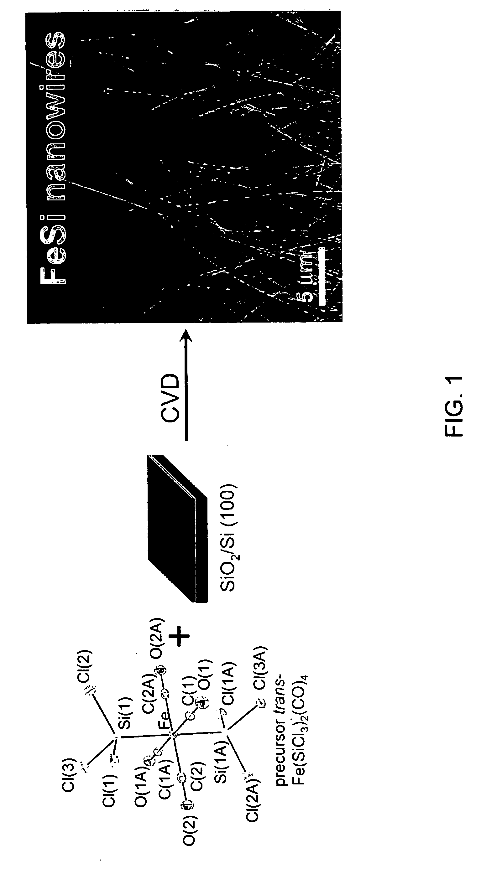
Unbranched FeSi Nanowires

[0039]Precursor Formation: The metal carbonyl-silyl organometallic single source precursor, Fe(SiCl3)2(CO)4 was synthesized from Fe3(CO)12 and SiHCl3 following a procedure modified from Novak et al., Organometallics, 16, 1567 (1997), the entire disclosure of which is incorporated herein by reference. Briefly, SiHCl3 (Aldrich, ca. 10 mL, 99 mmol) and Fe3(CO)12 (Aldirch, 0.998 g, 1.98 mmol) were loaded into a thick-walled glass tube equipped with a Teflon valve and pumped down to 0.5 Torr. The sealed vessel was then heated at 120° C. under stirring for 2 days during which the color of the solution turned from green to orange within the first hour. Warning: Heating volatile liquid reaction mixture that generates gas in close containers can cause pressure built up and potential explosion! After cooling, the reaction mixture was transferred to a sublimation apparatus in a nitrogen filled glove box. Excess SiHCl3 was removed under dynamic vacuum and the resulting ...

example 2

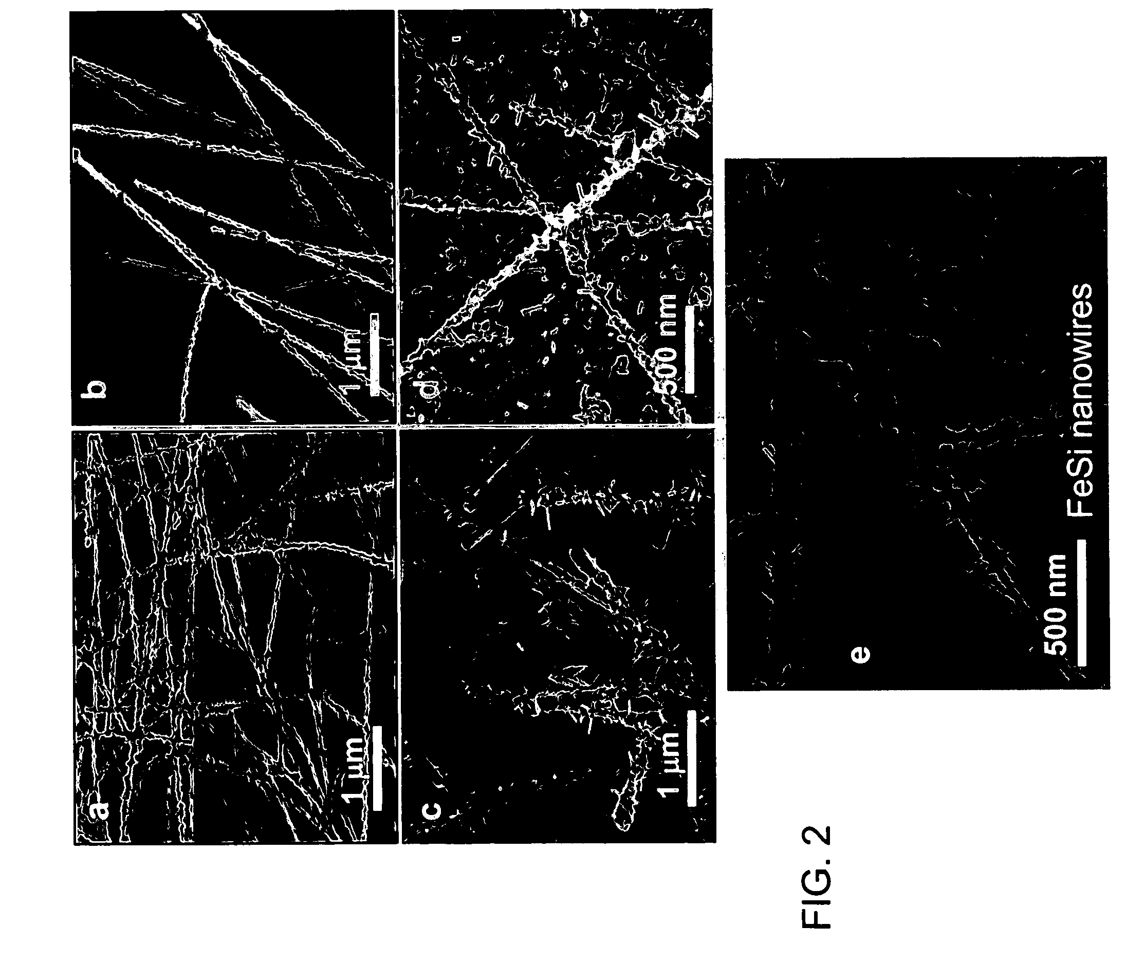
Branched FeSi Nanowires

[0043]Nanowire Formation: FeSi nanowires were produced using the CVD method described in Example 1, except that the oxide layers on the silicon substrates were reduced. To produce the silicon oxide coated substrates, all of the substrates were first etch with HF to remove native oxide and then: 1) exposed to a “metal etch” solution (30% H2O2: 37% HCl: H2O=1:1:5 v / v) at 70° C. for 3 or 7 minutes; 2) exposed to ambient air at room temperature for 1 day followed by vacuum annealing at 500° C. for 30 min; or 3) exposed to ambient air at room temperature for 4 days.

[0044]Nanowire Characterization: SEM images of the nanowires showed that the nanowires were branched with secondary nanowires or nanorods extending outwardly along the length of the main nanowire. The secondary structures are shown in FIG. 2, which shows SEM images of the nanowires grown on a silicon substrate that was teched with HF and then: (a) exposed to the metal etch solution for 3 min.; (b) expose...

example 3

CoSi Nanowires

[0045]Precursor Formation: In a typical synthesis of the metal carbonyl-silyl organometallic single source precursor, Co(SiCl3)(CO)4, approximately 15 ml of SiHCl3 was added to 3.04 g of dry Co2(CO)8 placed in a Carius tube and cooled to −40° C. in an acetonitrile / dry ice slurry. The reaction tube was pumped down to 0.5 Torr, sealed and stirred at −40° C. for 2 hours before warming to room temperature. The reaction mixture was transferred to a sublimation apparatus in a glove box and the remaining SiHCl3 was removed with dynamic vacuum before sublimation at 40° C. and 0.1 Torr was carried out for 2 hours. The final product of yellow crystals collected on the cold finger weighed 3.65 g (a 68% yield). Sublimed crystals were suitable for single crystal X-ray diffraction study, which revealed identical cell parameters to those previously reported.

[0046]Nanowire Formation: CoSi nanowire formation was carried out using the equipment and procedure of Example 1, above, with th...


PUM

PropertyMeasurementUnit
thicknessaaaaaaaaaa
diameteraaaaaaaaaa
thicknessaaaaaaaaaa

Abstract

The present invention provides metal silicide nanowires, including metallic, semiconducting, and ferromagnetic semiconducting transition metal silicide nanowires. The nanowires are grown using either chemical vapor deposition (CVD) or chemical vapor transport (CVT) on silicon substrates covered with a thin silicon oxide film, the oxide film desirably having a thickness of no greater than about 5 nm and, desirably, no more than about 2 nm (e.g., about 1-2 nm). The metal silicide nanowires and heterostructures made from the nanowires are well-suited for use in CMOS compatible wire-like electronic, photonic, and spintronic devices.

Description

FIELD OF THE INVENTION[0001]The present invention relates generally to the field of metal silicide nanowires and metal silicide nanowire synthesis.BACKGROUND OF THE INVENTION[0002]As MOSFET devices are scaled down smaller and smaller in ultra large scale integration (ULSI) processes, all aspects of the MOSFET device structures, including semiconductor channels, source and drain electrical contacts, gate stacks, and interconnects, need to be scaled. Increasingly, the now famous Moore's law has also become applicable to novel materials. Very prominent among these novel materials are metal silicides. Metal silicides are already of paramount importance as integral parts of silicon microelectronics, mainly because of the low resistivity ohmic contact to CMOS transistors provided by metallic silicides such as NiSi, CoSi2, and TiSi2 in the now dominant SALICIDE (Self-Aligned Silicides) process. In the last few years, metallic silicides, particularly nickel silicides (NiSi, Ni2Si, Ni3Si) ha...

Claims


Application Information

Patent Timeline
Patent Type & Authority Applications(United States)
IPC IPC(8): H01L23/532H01L21/3205H01L21/336
CPCH01L21/2855H01L21/28556H01L21/32053H01L23/53271H01L29/0657H01L29/0669H01L29/0673H01L2221/1094H01L29/4975H01L2924/0002H01L2924/00Y10T428/12431Y10T428/298
Inventor JIN, SONGSCHMITT, ANDREW L.SONG, YIPU
Owner WISCONSIN ALUMNI RES FOUND
Learn More