
Noncrystalline oxide semiconductor thin film, process for producing the noncrystalline oxide semiconductor thin film, process for producing thin-film transistor, field-effect-transistor, light emitting device, display device, and sputtering target

a technology of noncrystalline oxide and semiconductor, applied in the direction of metallic material coating process, solid-state device, diaphragm, etc., can solve the problems of difficult wet etching of oxide semiconductor itself, difficult to achieve large-scale and large-scale production, and difficult to pattern an electrode on an active layer, etc., to achieve easy to obtain large-area uniformity, improve the quality of large-size tft substrate, and increase the resistance to amorphous thin film

Active Publication Date: 2010-06-24
IDEMITSU KOSAN CO LTD
View PDF7 Cites 198 Cited by
  • Summary
  • Abstract
  • Description
  • Claims
  • Application Information

AI Technical Summary

Benefits of technology

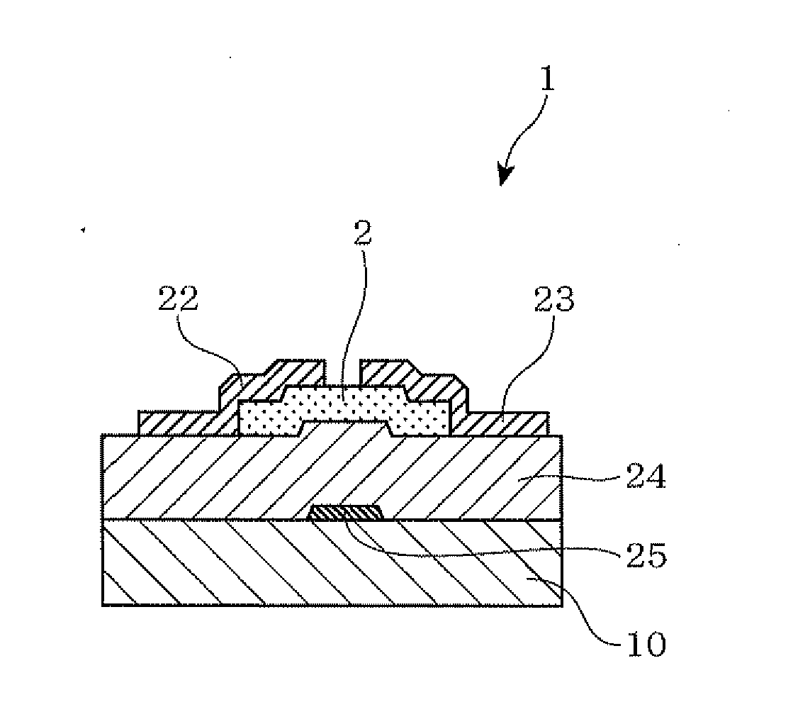
[0222]Materials for the gate insulating film 24 are not particularly limited, and materials generally used can be optionally selected within a range that the effects of the invention according to this embodiment are not lost, For instance, oxides such as SiO2, SiNx, Al2O3, Ta2O5, TiO2, MgO, ZrO2, CeO2, K2O, Li2O, Na2O, Rb2O, Sc2O3, Y2O3, Hf2O3, CaHfO3, PbTi3, BaTa2O6, SrTiO3 and AIN can be used. Of these, SiO2, SiNx, Al2O3, Y2O3, Hf2O3 and CaHfO3 are preferably used, more preferred are SiO2, SiNx, Y2O3, Hf2O3 and CaHfO3, and particularly preferred is Y2O3. The number of oxygen in these oxides does not necessarily agreed with its stoichiometric ratio (not only SiO2 but also SiOx are included, for example).
[0223]The gate insulating film 24 has a structure in which two or more different insulating films are stacked, though it is not shown in the drawing. Further, the gate insulating film 24 may be crystalline, polycrystalline or amorphous. However, polycrystalline and amorphous one are preferred which are industrially produced with ease.
[0224]The ratio of a channel width W and a channel length L W / L of the above-mentioned top-gate type thin film transistor 1a is normally 0.1 to 100, preferably 1 to 20, and particularly preferably 2 to 8. The reason therefor is that if the W / L exceeds 100, the amount of leakage current may increase or the on-off ratio may be lowered. If the W / L is smaller than 0.1, the field-effect mobility may be lowered or the pinch-off may be unclear.
[0225]Further, the channel length L is normally 0.1 to 1000 μm, preferably 1 to 100 μm, and further preferably 2 to 10 μm. The reason therefor is that if the channel length is less than 0.1 μm, production on the industrial basis may be difficult, or the amount of leakage current may increase. On the other hand, the channel length which exceeds 1000 μm is not preferable, since a device to be produced may become too large in size.
[0226]The thickness of the amorphous oxide semiconductor thin film 2 is normally 0.5 to 500 nm, preferably 1 to 150 nm, more preferably 3 to 80 nm, and particularly preferably 10 to 60 nm. This reason therefor is that if the thickness is smaller than 0.5 nm, it will become difficult to form a film uniformly on the industrial basis. On the other hand, if the thickness is larger than 500 nm, the time required for film-forming is too long to be industrially implemented. Further, if the thickness is within a range of 3 to 80 nm, the TFT characteristics such as mobility and an on-off ratio are particularly improved.
[0227]The field-effect mobility of the bottom-gate type thin film transistor 1 is typically 1 cm2 / Vs or more. If the field-effect mobility is less than 1 cm2 / Vs, a switching speed may be later. To effectively avoid such a defect, the field-effect mobility is preferably 5 cm2 / Vs or more, more preferably 18 cm2 / Vs or more, further preferably 30 cm2 / Vs or more, and particularly preferably 50 cm2 / Vs or more.

Problems solved by technology

Therefore, it was difficult to pattern an electrode on an active layer using such an oxide semiconductor by the photolithography method using wet etching.
Thus, it is necessary to employ a method like the liftoff method, which includes many steps and give a lower yield, as well as by which high resolution, large scale and production in large quantities are difficult to accomplish (see Patent Documents 1 and 6).
Although there is an oxide semiconductor which becomes insoluble in an etching solution used for forming a metal electrode, like PAN, by crystallization, it is difficult to wet etch the oxide semiconductor itself and the crystallization conditions are complicated.

Method used


Image

  • Noncrystalline oxide semiconductor thin film, process for producing the noncrystalline oxide semiconductor thin film, process for producing thin-film transistor, field-effect-transistor, light emitting device, display device, and sputtering target
  • Noncrystalline oxide semiconductor thin film, process for producing the noncrystalline oxide semiconductor thin film, process for producing thin-film transistor, field-effect-transistor, light emitting device, display device, and sputtering target
  • Noncrystalline oxide semiconductor thin film, process for producing the noncrystalline oxide semiconductor thin film, process for producing thin-film transistor, field-effect-transistor, light emitting device, display device, and sputtering target

Examples


example 1

(1) Production and Evaluation of Sputtering Target

1. Production of Target

[0132]As the raw materials, indium oxide powder, tin oxide powder and zinc oxide powder were mixed such that [In] / ([In]+[Sn]+[Zn]) was 0.20, [Sn] / ([In]+[Sn]+[Zn]) was 0.15, and [Zn] / ([In]+[Sn]+[Zn]) was 0.65. The mixture was then supplied to a wet ball mill and mixed and pulverized for about 72 hours, whereby raw material fine powder was obtained.

[0133]After granulating the raw material fine powders, the raw material fine powder was press-molded to have a diameter of 10 cm and a thickness of 5 mm. The molded product was put in a firing furnace, and firing was performed at 1400° C. for 48 hours to obtain a sintered body (target). The heating rate was 3° C. / min.

2. Evaluation of Target

[0134]For the resulting target, the density and the bulk resistance were measured. As a result, it was found that the theoretical relative density was 98% and the bulk resistance value measured by the four probe method was 80 mΩ.

(2) ...

example 2

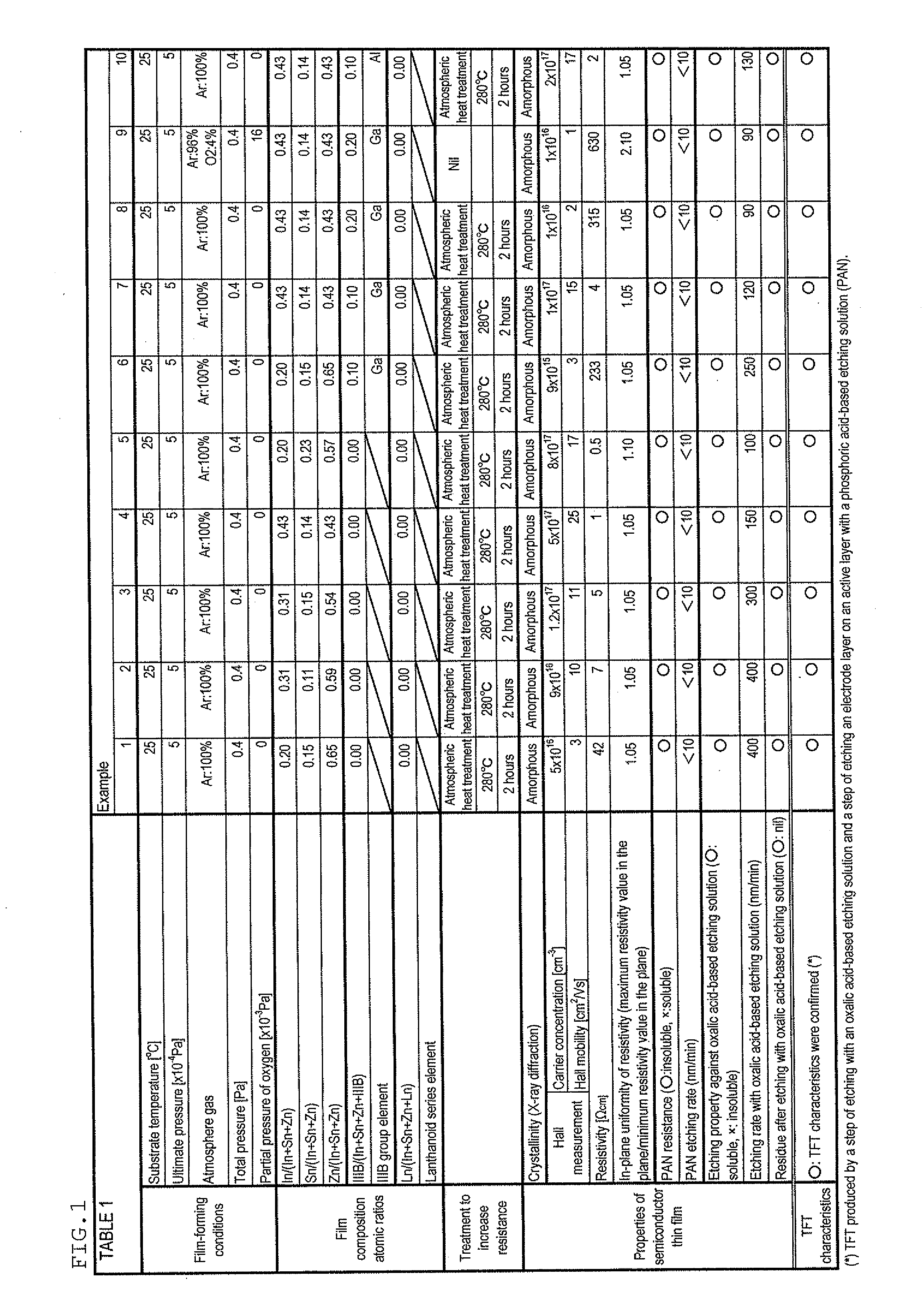
[0150]The amorphous oxide semiconductor thin film of Example 2 was produced in about the same manner as in Example 1 (film-forming conditions, film composition atomic ratios and treatment to increase resistance). The film composition was analyzed by the ICP method to find that the [In] / ([In]+[Sn]+[Zn]) was 0.31, the [Sn] / ([In]+[Sn]+[Zn]) was 0.11 and the [Zn] / ([In]+[Sn]+[Zn]) was 0.59.

[0151]The oxide semiconductor thin film produced under the above-mentioned production conditions has the properties as indicated in FIG. 1. It was found that the crystallinity was amorphous, the carrier concentration was 9×1016 cm−3, and the Hall mobility was 10 cm2 / Vs. The resistivity measured by the four probe method was 7 Ωcm. The in-plane uniformity of resistivity (maximum resistivity value in the plane / minimum resistivity value in the plane) was 1.05. The etching rate with the PAN etching solution was less than 10 nm / min, and the evaluation was good (insoluble). The etching rate with the oxalic ac...

example 3

[0152]The amorphous oxide semiconductor thin film of Example 3 was produced in about the same manner as in Example 1 (film-forming conditions, film composition atomic ratios and treatment to increase resistance). The film composition was analyzed by the ICP method to find that the [In] / [In]+[Sn]+[Zn]) was 0.31, the [Sn] / ([In]+[Sn]+[Zn]) was 0.15, and the [Zn] / [In]+[Sn]+[Zn]) was 0.54.

[0153]The oxide semiconductor thin film produced under the above-mentioned production conditions has the properties as indicated in FIG. 1. It was found that the crystallinity was amorphous, the carrier concentration was 1.2×1017 cm−3, and the Hall mobility was 11 cm2 / Vs. The resistivity measured by the four probe method was 5 Ωcm. The in-plane uniformity of resistivity (maximum resistivity value in the plane / minimum resistivity value in the plane) was 1.05. The etching rate with the PAN etching solution was less than 10 nm / min, and the evaluation was good (insoluble). The etching rate with the oxalic a...


PUM

PropertyMeasurementUnit
Temperatureaaaaaaaaaa

Abstract

This invention provides an amorphous oxide semiconductor thin film, which is insoluble in a phosphoric acid-based etching solution and is soluble in an oxalic acid-based etching solution by optimizing the amounts of indium, tin, and zinc, a method of producing the amorphous oxide semiconductor thin film, etc. An image display device (1) comprises a glass substrate (10), a liquid crystal (40) as a light control element, a bottom gate-type thin film transistor (1) for driving the liquid crystal (40), a pixel electrode (30), and an opposing electrode (50). The amorphous oxide semiconductor thin film (2) in the bottom gate-type thin film transistor (1) has a carrier density of less than 10+18 cm−3, is insoluble in a phosphoric acid-based etching liquid, and is soluble in an oxalic acid-based etching liquid.

Description

[0001]TECHNICAL FIELD[0002]The invention relates to an amorphous oxide semiconductor thin film, a method of producing the same, a method of producing a thin film transistor, a field-effect type transistor, a light-emitting apparatus, a display apparatus and a sputtering target. In particular, the invention relates to an amorphous oxide semiconductor thin film which has a carrier density of less than 10+18 cm−3, is insoluble in a phosphoric acid-based etching solution, and is soluble in an oxalic acid-based etching solution, a method of producing the same, and the like.BACKGROUND ART[0003]Active matrix type image display apparatuses such LCD (liquid crystal display apparatus) and an organic EL (Electro Luminescence) display apparatus have been widely used because of their display performance, energy saving, etc. Such active matrix type display apparatuses have been mainstream display apparatuses for mobile phones, PDAs (Personal Digital Assistant), personal computers, laptop personal...

Claims


Application Information

Patent Timeline
IPC IPC(8): H01L29/24H01L21/302H01L29/04H01L29/78H01L33/26H01L21/477C23C14/34
CPCC23C14/086H01L29/66969C23C14/3492H01L21/02554H01L21/02565H01L21/02592H01L21/02631H01L21/32134H01L27/1225H01L29/45H01L29/7869C04B35/453C04B35/6261C04B2235/3224C04B2235/3227C04B2235/3229C04B2235/3284C04B2235/3286C04B2235/3293C04B2235/6562C04B2235/77C23C14/3414
Inventor YANO, KOKIINOUE, KAZUYOSHI
Owner IDEMITSU KOSAN CO LTD
Learn More