
L10-ORDERED FePt NANODOT ARRAY, METHOD OF MANUFACTURING THE SAME AND HIGH DENSITY MAGNETIC RECORDING MEDIUM USING THE SAME

a nanodot array and nanodot technology, applied in the field of l10-ordered fept nanodot array, can solve the problems of increasing manufacturing time, high probability of mold breaking, and increasing manufacturing period and cos

Inactive Publication Date: 2010-06-17
KOREA ADVANCED INST OF SCI & TECH
View PDF6 Cites 4 Cited by
  • Summary
  • Abstract
  • Description
  • Claims
  • Application Information

AI Technical Summary

Problems solved by technology

However, whenever manufacturing the nanodot-patterned recording media, e-beam lithography or holographic lithography applying expensive equipment should be used, undesirably increasing the manufacturing period and cost.
However, this method is problematic because a typical silicon mold should be designed using e-beam lithography to obtain a pattern on the nano scale, thus increasing the manufacturing time compared to when using injection molding and resulting in high probability of breaking the mold.

Method used


Image

  • L10-ORDERED FePt NANODOT ARRAY, METHOD OF MANUFACTURING THE SAME AND HIGH DENSITY MAGNETIC RECORDING MEDIUM USING THE SAME
  • L10-ORDERED FePt NANODOT ARRAY, METHOD OF MANUFACTURING THE SAME AND HIGH DENSITY MAGNETIC RECORDING MEDIUM USING THE SAME
  • L10-ORDERED FePt NANODOT ARRAY, METHOD OF MANUFACTURING THE SAME AND HIGH DENSITY MAGNETIC RECORDING MEDIUM USING THE SAME

Examples


Embodiment Construction

[0036]Hereinafter, a detailed description will be given of embodiments of the present invention with reference to the accompanying drawings. Throughout the drawings, the same reference numerals refer to the same or similar elements. In the description, the detailed descriptions of known techniques pertaining to the present invention are omitted so as not to make the characteristics of the invention unclear.

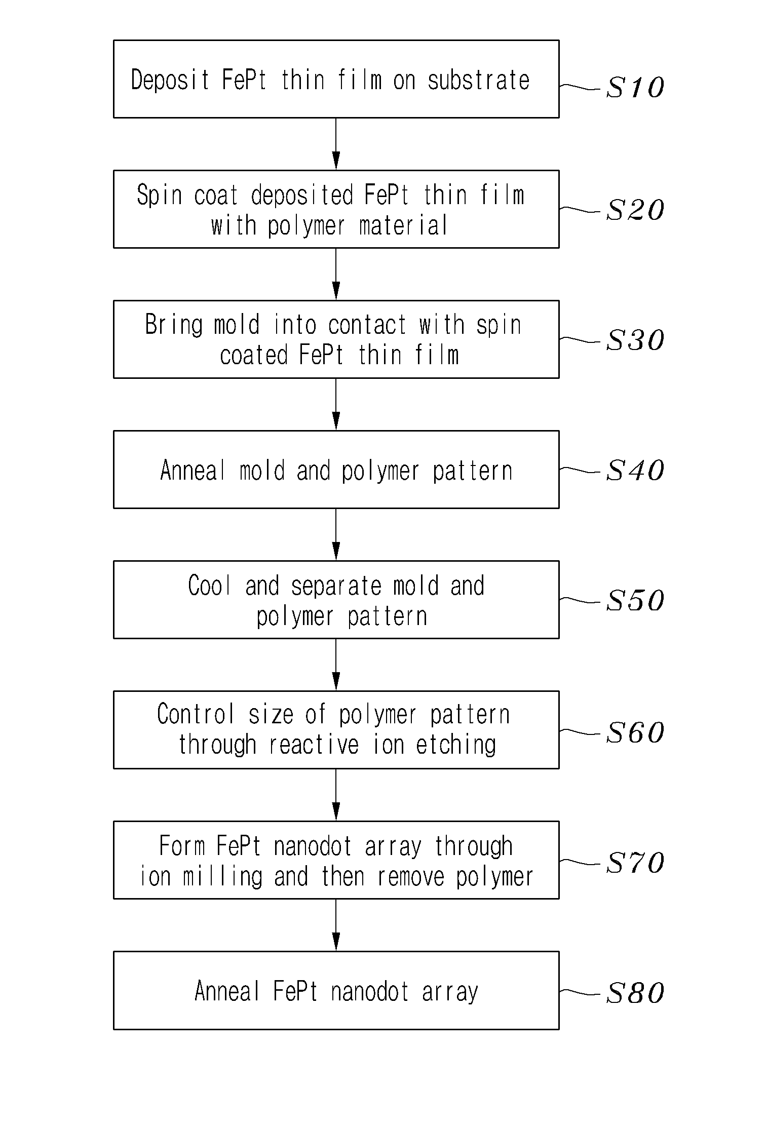
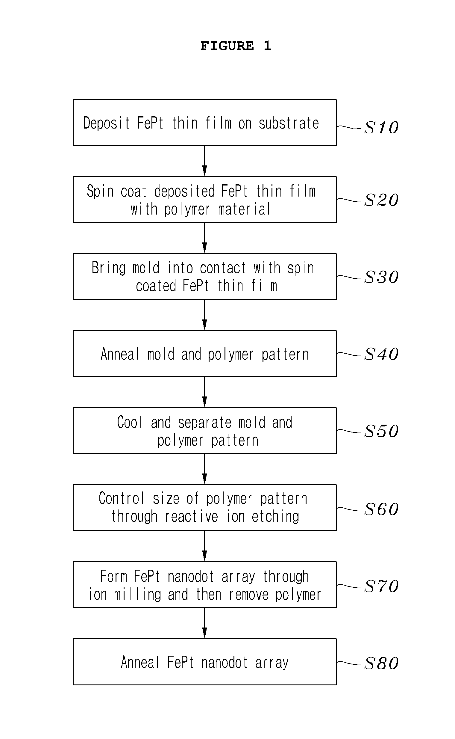
[0037]FIG. 1 is a flowchart showing a process of manufacturing a patterned FePt nanodot array according to an embodiment of the present invention. As shown in FIG. 1, the method of manufacturing the patterned FePt nanodot array according to the present invention includes S10 to S80, which are stepwisely specified below.

[0038]S10 is a process of depositing a FePt thin film on a MgO substrate.

[0039]The FePt thin film may be deposited through sputtering. In the present invention, DC magnetron sputtering is employed.

[0040]Alternatively, in lieu of DC magnetron sputtering, a deposition...


PUM

PropertyMeasurementUnit
thicknessaaaaaaaaaa
sizeaaaaaaaaaa
sizeaaaaaaaaaa

Abstract

This invention relates to a L10-ordered FePt nanodot array which is manufactured using capillary force lithography, to a method of manufacturing the L10-ordered FePt nanodot array and to a high density magnetic recording medium using the L10-ordered FePt nanodot array. This method includes depositing a FePt thin film on a MgO substrate, forming a thin film made of a polymer material on the deposited FePt thin film using spin coating, bringing a mold into contact with the spin coated FePt thin film, annealing the mold and a polymer pattern which are in contact with each other, cooling and separating the mold and the polymer pattern which are annealed, controlling a size of the polymer pattern through reactive ion etching, ion milling a portion of the FePt thin film uncovered with the polymer pattern thus forming a FePt nanodot array and then removing a remaining polymer layer, and annealing the FePt nanodot array.

Description

RELATED APPLICATIONS[0001]This patent application claims the benefit of priority under 35 U.S.C. §119 from Korean Patent Application No. 10-2008-0125792 filed Dec. 11, 2008, the contents of which are incorporated herein by reference.BACKGROUND OF THE INVENTION[0002]1. Field of the Invention[0003]The present invention relates to a L10-ordered FePt nanodot array, a method of manufacturing the same and a patterned high density magnetic recording medium using the same, and more particularly, to a patterned nanodot array adapted for recording media having ultrahigh density of at least terabits per square inch.[0004]2. Description of the Related Art[0005]With the acceleration of digital technology and the drastic increase in the amount of information available online, the demand for storage media having a reduced bit size, i.e. storage media having high recording density per unit area, is increasing in the market.[0006]Examples of a non-volatile storage method may include magnetic recordi...

Claims


Application Information

Patent Timeline
Patent Type & Authority Applications(United States)
IPC IPC(8): G11B5/65B32B37/00B32B38/10C21D1/00B32B3/00
CPCB82Y25/00G11B5/855H01F1/009Y10T428/24612H01F41/18H01F1/068H01F1/065G11B5/84G11B5/74B82Y40/00
Inventor SHIN, SUNG CHULJUNG, HEE-TAEKO, HYUN-SEOKJUNG, JIN-MI
Owner KOREA ADVANCED INST OF SCI & TECH
Learn More