
Planar waveguide wavelength dispersive devices with multiple waveguide input aperture

a waveguide and wavelength dispersive technology, applied in the field of waveguide based spectrometers, can solve the problems of insufficient light throughput, reduced light throughput (étendue), and even more obvious problems, and achieve the effects of compact layout, simple readout method, and large optical throughpu

Active Publication Date: 2010-05-06
NAT RES COUNCIL OF CANADA
View PDF11 Cites 22 Cited by
  • Summary
  • Abstract
  • Description
  • Claims
  • Application Information

AI Technical Summary

Benefits of technology

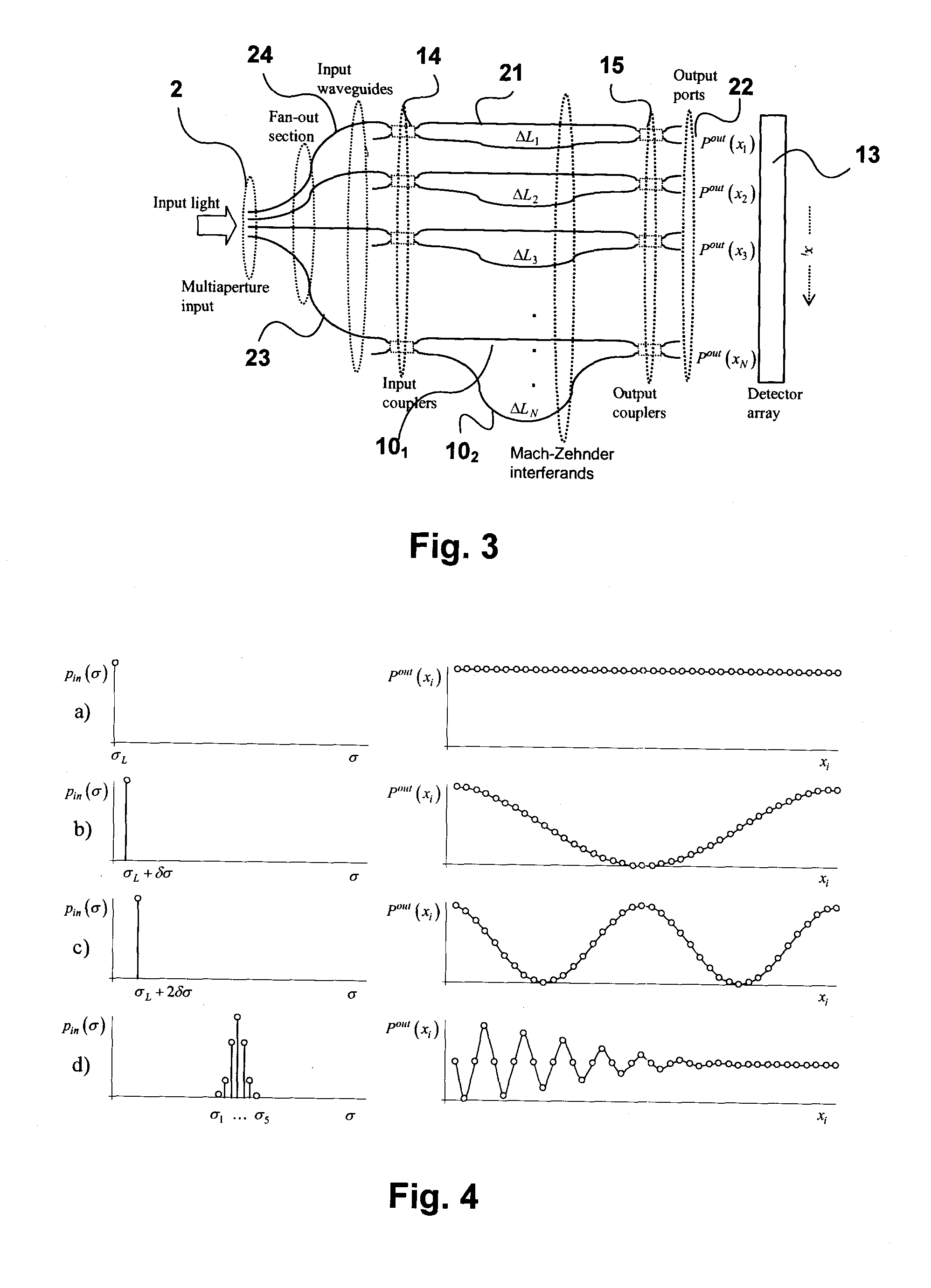
[0013]The use of a multi-input aperture input solves the problem of etendue because it allows the spectrometer to be used with spatially extended light source and thus maximizes the total light gathering capacity. Unlike the case of an conventional arrayed waveguide spectrometer, for example, the incoming light does not need to be focused on to a small aperture.
[0018]It is another object of the invention to relax the fabrication tolerances on waveguide lengths and optical path errors.
[0020]Embodiments of the invention contribute to the reduction of errors by permitting simple software calibration. Embodiments of the invention also provide optical apodization by simple software calibration.
[0022]Embodiments of the invention offer a larger optical throughput and a compact layout, and a simpler readout method.
[0023]Spectrometers in accordance with the invention can be made using standard waveguide fabrication techniques to provide a robust device.

Problems solved by technology

However, a reduction in the input aperture invariably results in a reduced light throughput (étendue) because of a degraded light coupling efficiency between the delivery system (typically an optical fiber) and the spectrometer.
The problem is even more obvious when using optical fibers with large core area (multimode fibers).
In addition to these étendue concerns, it is known that the input waveguide width cannot be reduced below the point at which the confinement of the mode is compromised and mode delocalization occurs.
This sets an ultimate limit to a grating-based waveguide spectrometer resolution.
However, virtually all of these spectrometers suffer from a limited resolution (typically >1 nm) which is not suitable for high resolution spectroscopies.
Even to achieve a moderate performance, including resolution and light gathering capability (étendue), serious fabrication difficulties have to be resolved.
Waveguide inhomogeneities during embossing induce a significant stray light level compromising resolution and crosstalk, and reducing detection accuracy particularly in spectral ranges of low sensitivity.
The latter is due to difficulties with fabrication of micro-mirror surfaces with high surface quality, parallelism and reflectivity.
Commercial portable micro-spectrometer systems exist, such as the Ocean Optics S1000 and S2000 series, the microParts LIGA serie, the Carl Zeiss MMS1, IOSPEC by MPB Technologies, and the Elargen micro-lightguide spectrometer, but their use is again limited to spectroscopic application with low resolution.
Increasing the resolution in these devices is inevitably accompanied by degrading light throughput rendering these devices useless for high-sensitivity high-resolution applications.
Unfortunately, typical FT spectrometers require moving parts, which is very difficult to realize in an integrated optics version, although recently, a new FT spatial heterodyne spectrometer with no need for moving part has been demonstrated both in bulk optics and planar waveguide form.
As such they are large and require careful assembly for each device.
The actual physical layout of the device is somewhat complex and involves making compromises in resolving power, etendue and size to get a working device.
In echelle waveguide grating devices, some complex fabrication steps are required to create waveguide vertical trenches with smooth vertical sidewalls.

Method used


Image

  • Planar waveguide wavelength dispersive devices with multiple waveguide input aperture
  • Planar waveguide wavelength dispersive devices with multiple waveguide input aperture
  • Planar waveguide wavelength dispersive devices with multiple waveguide input aperture

Examples


Embodiment Construction

[0044]The above mentioned drawbacks can be overcome by using a spectrometer with multiple input waveguides. Intercepting incoming light by multiple input waveguides allows maximizing total light gathering capability (étendue).

[0045]The spectrometer shown in FIG. 1 in schematic form comprises two interleaved waveguide arrays 8, 9 formed by alternate waveguide elements 10 constructed in a slab waveguide. The waveguides of the first array 8 introduce a delay 10a, which progressively increases across the array while the waveguides of the second array 8, introduce a delay 10b, which progressively decreases across the array in a complementary manner, so that the arrays create interference orders m and −m, respectively, thus combining two dispersive systems of opposite signs. The adjacent waveguide pairs can also be considered as individual waveguide structures forming interferometers, the outputs of which are superimposed to form output wavefronts 11, 12 which are detected by photodetecto...


PUM


Abstract

A spectrometer has a multi-input aperture for admitting an input wavefront and an array of multiple waveguide structures terminating at the multi-input aperture. The input wavefront is incident on each of the waveguide structures, which provide a dispersive function for the input wavefront. Interferometers are formed by elements of the waveguide structures. The interferometers have different optical path length differences (OPDs). The interferometers provide a wavelength responsive output for spatially extended light sources. The output of the interferometers is detected with a detector array. The spectrometer has an improved etendue, and in some embodiments very high resolution.

Description

CROSS REFERENCE TO RELATED APPLICATION[0001]This application claims the benefit under 35 USC 119(e) of prior U.S. application Nos. 60 / 907,127, filed Mar. 22, 2007 and 60 / 935,554, filed Aug. 17, 2007, the contents of which are herein incorporated by reference.FIELD OF THE INVENTION[0002]This application relates to spectrometers and more specifically to waveguide based spectrometers.BACKGROUND[0003]Waveguide-based spectrometers capable of separating light signals at different wavelengths have already been established as one of the key technologies in wavelength division multiplexed telecommunications networks (wavelength multiplexers and demultiplexers, add-drop filters, channel monitors, etc.). High-resolution spectroscopic devices are also required for the development of new detection platforms for genomics and health related applications, and environmental monitoring, including space-born sensing.[0004]In grating spectrometers, high resolution is achieved by reducing the input slit...

Claims


Application Information

Patent Timeline
Patent Type & Authority Applications(United States)
IPC IPC(8): G01J3/45
CPCG01J3/02G01J3/0218G01J3/12G01J3/1895G01J3/26G01J3/4532G02B6/12007G02B6/12011G02B6/29301G02B6/29352G02B6/29356G02B6/4215
Inventor CHEBEN, PAVELJANZ, SIEGFRIEDFLORJANCZYK, MIROSLAWXU, DAN-XIA
Owner NAT RES COUNCIL OF CANADA
Learn More