Conductive laminated body and method for preparing the same
a technology of laminated body and conductive material, which is applied in the direction of conductors, natural mineral layered products, superimposed coating processes, etc., can solve the problems of uneven distribution of electrical properties, heat-resistance/moisture resistance of thin films, etc., to improve resistivity properties, reduce electron mobility, and increase electron concentration
- Summary
- Abstract
- Description
- Claims
- Application Information
AI Technical Summary
Benefits of technology
Problems solved by technology
Method used
Image
Examples
example 1
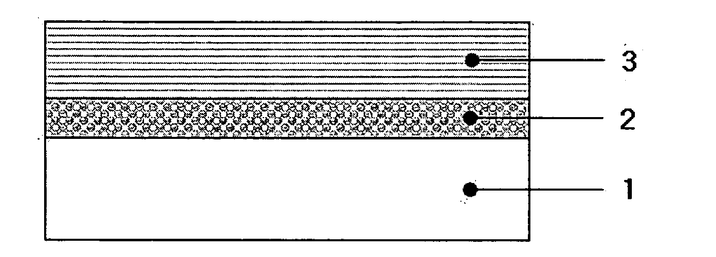
Preparation of a Conductive Laminated Body—Al Doped ZnO / Al2O3 Interlayer / Glass
[0069]Onto a glass substrate (TFT glass), an Al2O3 thin film was deposited by RF magnetron sputtering. As a sputtering target, an Al2O3 sintered body target was used, and three test samples of the deposited Al2O3 thin film of were prepared. Herein, the test samples had thickness of 19 nm, 20 nm, 32 nm, respectively.
[0070]In addition, bias voltage was about −350V, the pressure within a chamber was 3×10⁻³ torr, and the flow rate of argon gas was 50 sccm.
[0071]Onto the prepared Al2O3 interlayer, a ZnO (2 wt % of Al was doped) thin film was deposited by RF magnetron sputtering to obtain a conductive laminated body. As a sputtering target, a ZnO (2 wt % of Al was doped) sintered body target was used, and the thickness of the deposited ZnO thin film was 140 nm (±7 nm). Other sputtering conditions were the same as those of the deposition of the interlayer.
example 2
Preparation of a Conductive Laminated Body—Ga Doped ZnO / Ga2O3 Interlayer / Glass
[0072]A conductive laminated body was prepared in the same manner as described in Example 1, except that Ga2O3 was deposited as an interlayer, and 5.5 wt % of Ga was doped on ZnO.
example 3
Preparation of a Conductive Laminated Body—Ga Doped ZnO / Al2O3 Interlayer / Glass
[0073]A conductive laminated body was prepared in the same manner as described in Example 1, except that 5.5 wt % of Ga was doped on ZnO.
PUM
| Property | Measurement | Unit |
|---|---|---|
| thickness | aaaaa | aaaaa |
| temperature | aaaaa | aaaaa |
| vol % | aaaaa | aaaaa |
Abstract
Description
Claims
Application Information
 - R&D
- Intellectual Property
- Life Sciences
- Materials
- Tech Scout
- Unparalleled Data Quality
- Higher Quality Content
- 60% Fewer Hallucinations
Browse by: Latest US Patents, China's latest patents, Technical Efficacy Thesaurus, Application Domain, Technology Topic, Popular Technical Reports.
© 2025 PatSnap. All rights reserved.Legal|Privacy policy|Modern Slavery Act Transparency Statement|Sitemap|About US| Contact US: help@patsnap.com


