Memory and manufacturing method thereof
一种存储器、氧化物的技术,应用在半导体/固态器件制造、电固体器件、半导体器件等方向,能够解决电子浓度降低、影响数据读取正确性、位错误等问题
- Summary
- Abstract
- Description
- Claims
- Application Information
AI Technical Summary
Problems solved by technology
Method used
Image

Examples
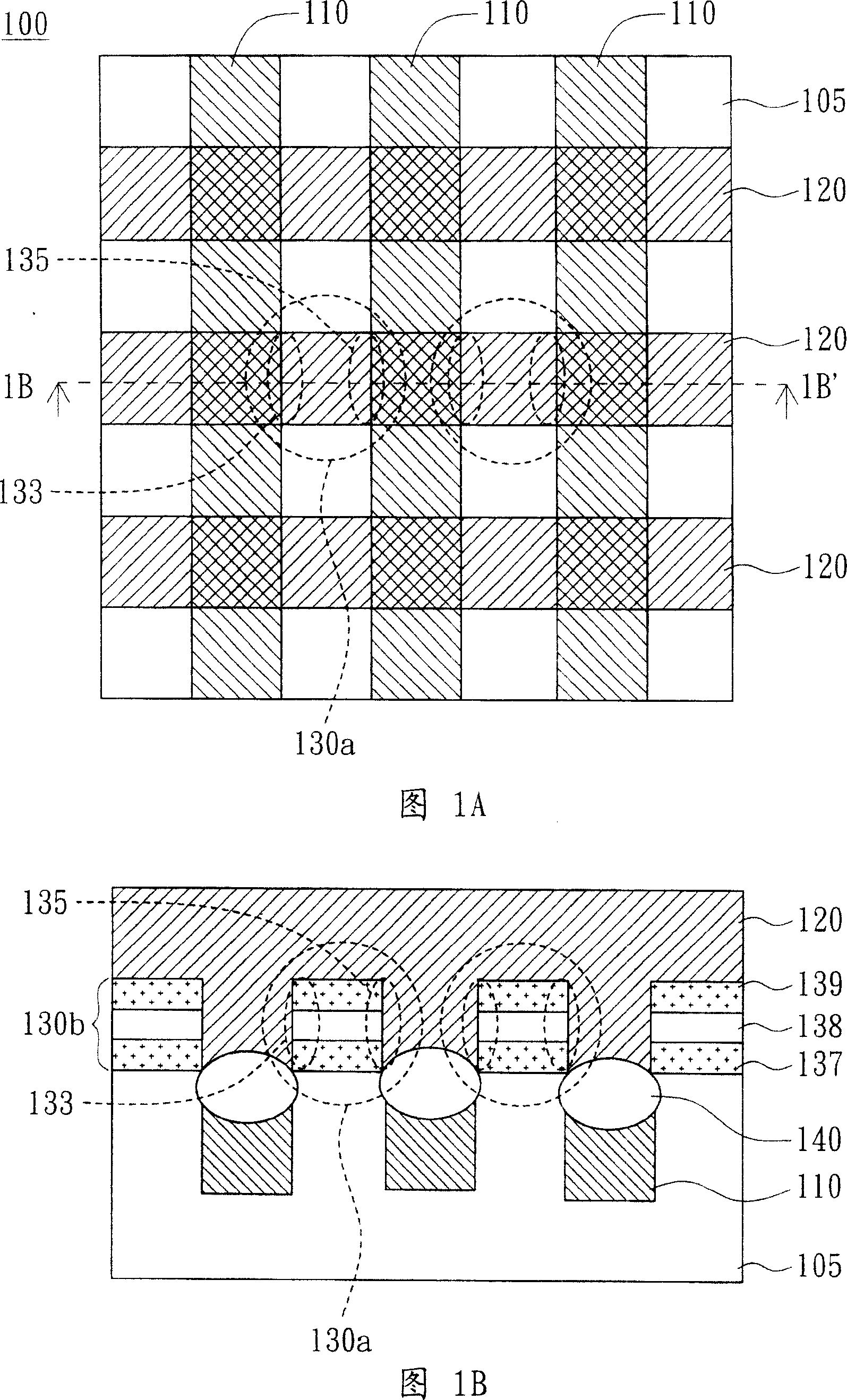
no. 1 example
[0038] Please refer to FIG. 2A and FIG. 2B at the same time. FIG. 2A shows a partial top view of the memory according to the first embodiment of the present invention, and FIG. 2B shows a cross-section of the memory along the section line 2B-2B' of FIG. 2A picture. 2A-2B, the memory 200 includes a substrate 210, a plurality of bit lines (bitlines) 220, a plurality of word lines (word lines) 230, a plurality of oxide / nitride / oxide (oxide-nitride-oxide, ONO) stack structure 240, a plurality of spacer layers 250, a plurality of storage units 215 (shown in larger dotted line ranges in FIG. 2A and FIG. 2B ), a plurality of first storage nodes (storagenode) 217a, a plurality of first Binary storage section 217b. The bit lines 220 are disposed parallel to each other in the substrate 210 and located near the surface of the substrate 210 . The word lines 230 are arranged parallel to each other on the substrate 210 , and the word lines 230 and the bit lines 220 cross each other, but t...
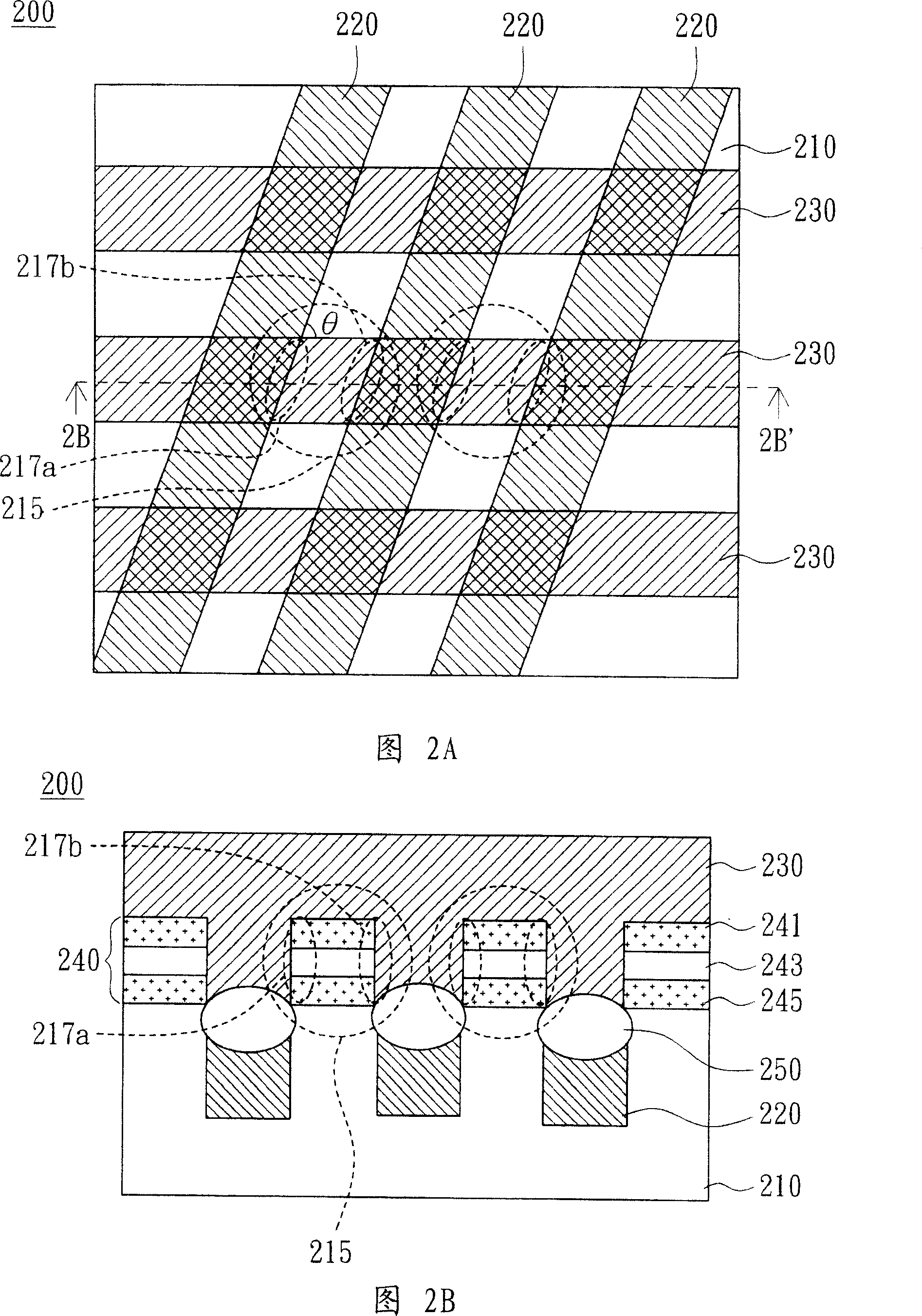
no. 2 example
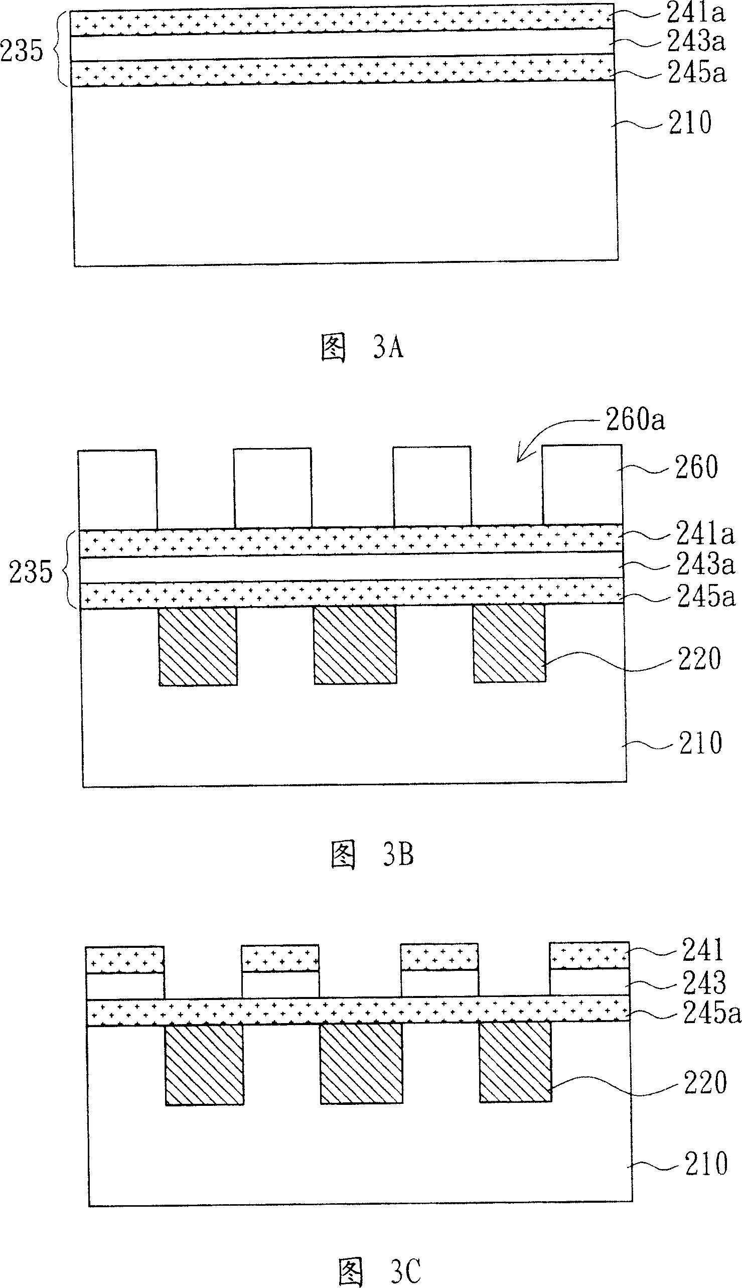
[0048] Please refer to FIG. 4A and FIG. 4B at the same time. FIG. 4A shows a partial top view of the memory according to the second embodiment of the present invention, and FIG. 4B shows a cross-section of the memory along the section line 4B-4B' of FIG. 4A picture. In FIGS. 4A-4B, the memory 300 includes a substrate 310, a plurality of bit lines 320, a plurality of word lines 330, an oxide / nitride / oxide (oxide-nitride-oxide, ONO) layer 340, a plurality of memory The unit 315 (as shown by the larger dotted line in FIG. 4A and FIG. 4B ), a plurality of first bit storage sections 317a, and a plurality of second bit storage sections 317b. The bit lines 320 are disposed parallel to each other in the substrate 310 and located near the surface of the substrate 310 . The word lines 330 are arranged parallel to each other on the substrate 310 , and the word lines 330 and the bit lines 320 cross each other, but the word lines 330 and the bit lines 320 are not perpendicular to each oth...
PUM
 Abstract
Description
Claims
Application Information
 - R&D
- Intellectual Property
- Life Sciences
- Materials
- Tech Scout
- Unparalleled Data Quality
- Higher Quality Content
- 60% Fewer Hallucinations
Browse by: Latest US Patents, China's latest patents, Technical Efficacy Thesaurus, Application Domain, Technology Topic, Popular Technical Reports.
© 2025 PatSnap. All rights reserved.Legal|Privacy policy|Modern Slavery Act Transparency Statement|Sitemap|About US| Contact US: help@patsnap.com