
Apparatus, Method and Computer Program Product for Fast Stimulation of Manufacturing Effects During Integrated Circuit Design

a technology of integrated circuit design and simulation, applied in the field of methods, apparatus and computer program products for simulating and designing integrated circuits, can solve the problems of significant challenges in applying these models to the design stage, increasing the influence of integrated circuit design, and still exist thickness variations

Inactive Publication Date: 2010-03-25
GLOBALFOUNDRIES INC
View PDF12 Cites 25 Cited by
  • Summary
  • Abstract
  • Description
  • Claims
  • Application Information

AI Technical Summary

Benefits of technology

[0011]The foregoing and other problems are overcome, and other advantages are realized, in accordance with the following embodiments of the invention.

Problems solved by technology

As CMOS technology continues to scale, integrated circuit designs are increasingly affected by the variability in the back end of the line.
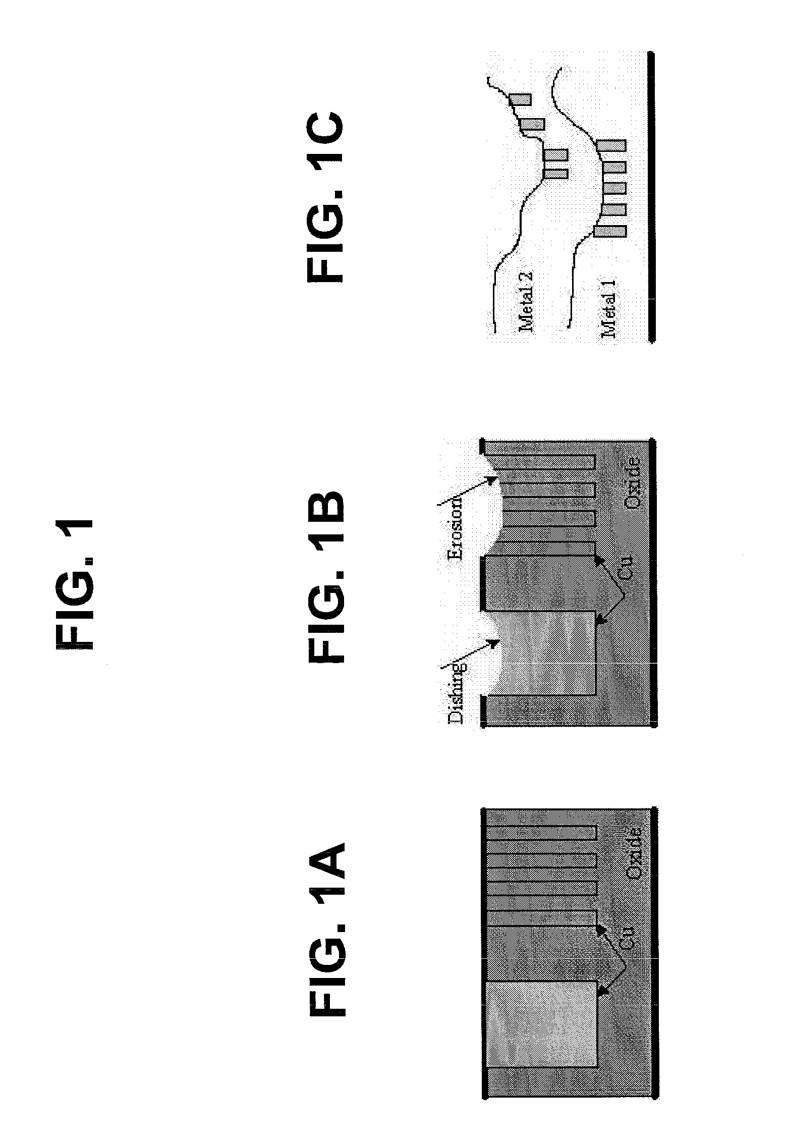
However, due to dishing and erosion, thickness variations still exist after a CMP process.
However, although several accurate CMP models exist, there are still significant challenges in applying these models to the design stage due to the following three reasons.
However, in large-scale integrated circuit designs, the hierarchical approach is widely adopted such that designers may work only on part of the design, and no full chip information is available.
Second, the execution time of a full chip CMP prediction is long, measured by hours.
However, the design process is an iterative process, and multiple iterations are required to refine and optimize the design.
A long execution time for a CMP model can greatly restrict its application in the design stage.
However, the CMP models have to consider the long range impacts, and will still take the full chip information for a full chip prediction, which takes a long time to complete.

Method used


Image

  • Apparatus, Method and Computer Program Product for Fast Stimulation of Manufacturing Effects During Integrated Circuit Design
  • Apparatus, Method and Computer Program Product for Fast Stimulation of Manufacturing Effects During Integrated Circuit Design
  • Apparatus, Method and Computer Program Product for Fast Stimulation of Manufacturing Effects During Integrated Circuit Design

Examples


Embodiment Construction

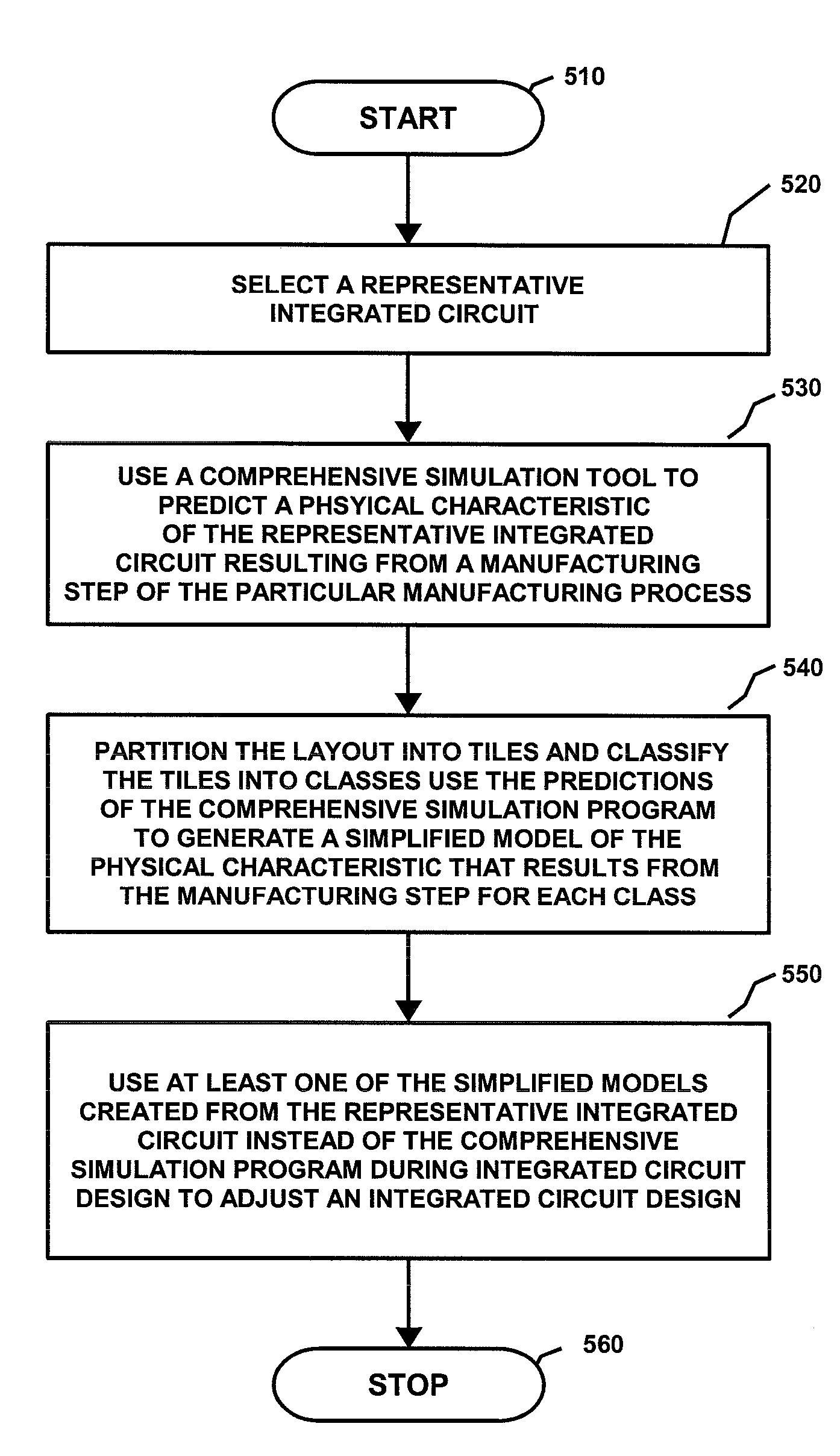
[0027]To address these issues in existing CMP models, the present invention uses a fast empirical CMP model based on simulation results from an industry CMP analysis tool, which does CMP predictions based on tile metrics (e.g., density, wire width, wire spacing, wire length etc.). The fast new model of the invention successfully addresses the above-identified three difficulties. The new model receives prefill (prehole) designs as input, and generates post fill (hole) thickness maps for copper interconnects. Accordingly, copper interconnect thickness can be calculated on each tile. This allows local changes to be well captured and easily updated.

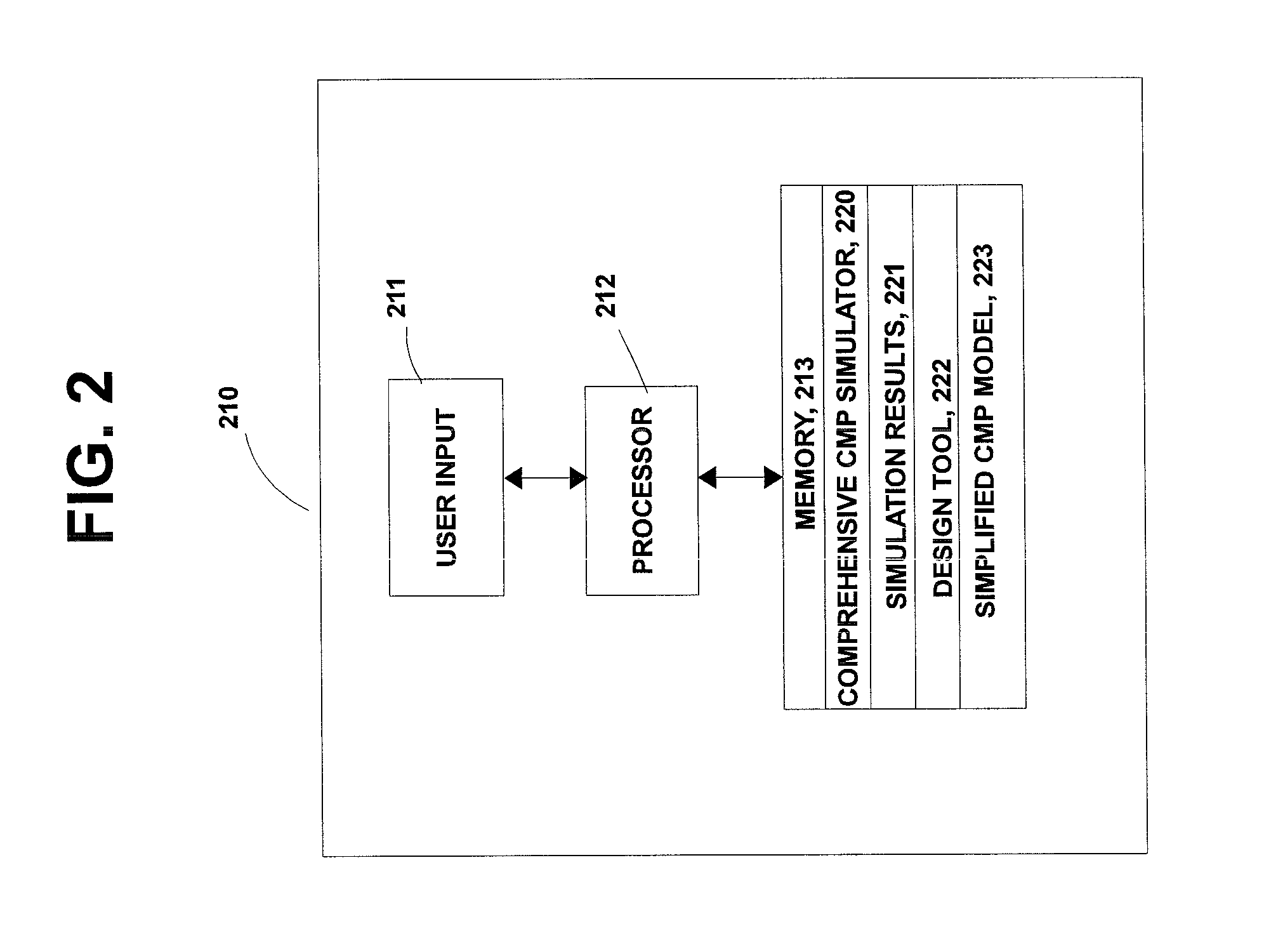
[0028]In the invention, an industry CMP analysis tool, which accurate provides full chip, multi-level topography predictions for copper ECD and CMP, is used to generate CMP simulation data for particular manufacturing processes. For this kind of CMP simulator, the simulation accuracy can be higher than 90% for 65 nm Cu CMP process. The simula...


PUM


Abstract

Methods, apparatus and computer program products provide a fast and accurate model for simulating the effects of chemical mechanical polishing (CMP) steps during fabrication of an integrated circuit by generating a design of an integrated circuit; while generating the design of the integrated circuit, using a simplified model to predict at least one physical characteristic of the integrated circuit which results from a CMP processing step to be used during manufacture of the integrated circuit, wherein the simplified model is derived from simulations performed prior to the design generation activities using a comprehensive simulation program used to model the physical characteristic; predicting performance of the integrated circuit using the predicted physical characteristic; and adjusting the design of the integrated circuit in dependence on the performance prediction.

Description

TECHNICAL FIELD[0001]The invention generally concerns methods, apparatus and computer program products for simulating and designing integrated circuits, and more particularly concerns methods, apparatus and computer program products for simulating the effects of fabrication processes on the electrical performance of integrated circuits during the design phase.BACKGROUND[0002]As CMOS technology continues to scale, integrated circuit designs are increasingly affected by the variability in the back end of the line. In order to achieve acceptable design quality, theses variations should be well understood so that their impact can be taken into account in circuit and layout design flow.[0003]Chemical Mechanical Planarization (“CMP”) is a primary technique to planarize layout surfaces in order to establish reliable multilevel copper interconnects, and constitutes one or more steps in a typical semiconductor manufacturing process. In modern manufacturing processes, after depositing a new l...

Claims


Application Information

Patent Timeline
Patent Type & Authority Applications(United States)
IPC IPC(8): G06F17/50
CPCG06F2217/12G06F17/5009G06F2119/18G06F30/20Y02P90/02G06F17/40
Inventor XIANG, HUAECONOMIKOS, LAERTISFAYAZ, MOHAMMED F.GRECO, STEPHEN E.O'NEIL, PATRICIA A.PURI, RUCHIR
Owner GLOBALFOUNDRIES INC
Learn More