
Patterning process

a pattern and pattern technology, applied in the field of patterning process, can solve the problems of reducing the lwr and reducing the dimension of the photoresist pattern, and achieve the effect of avoiding the deterioration of the photoresist profil

Active Publication Date: 2010-03-04
SHIN ETSU CHEM IND CO LTD
View PDF9 Cites 57 Cited by
  • Summary
  • Abstract
  • Description
  • Claims
  • Application Information

AI Technical Summary

Benefits of technology

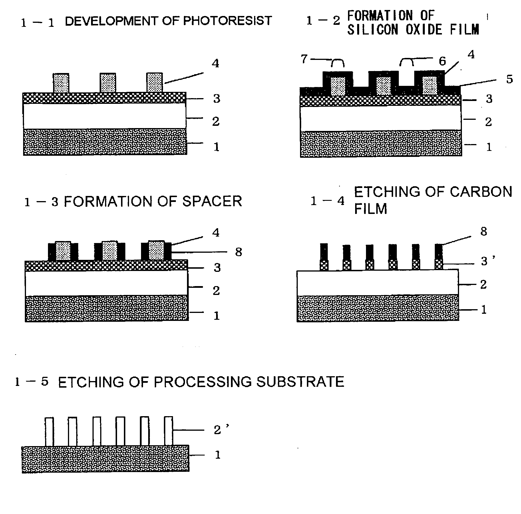
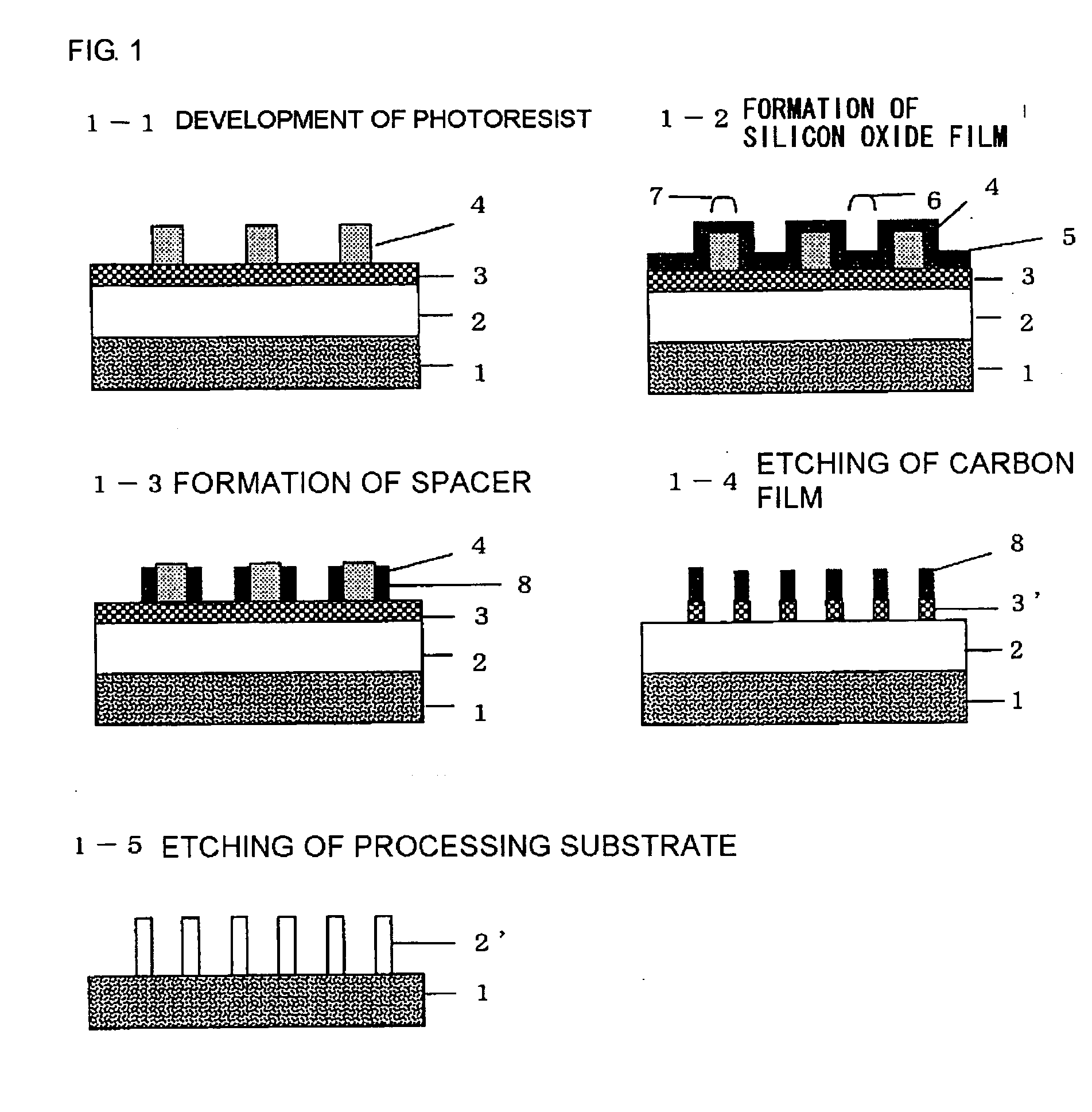
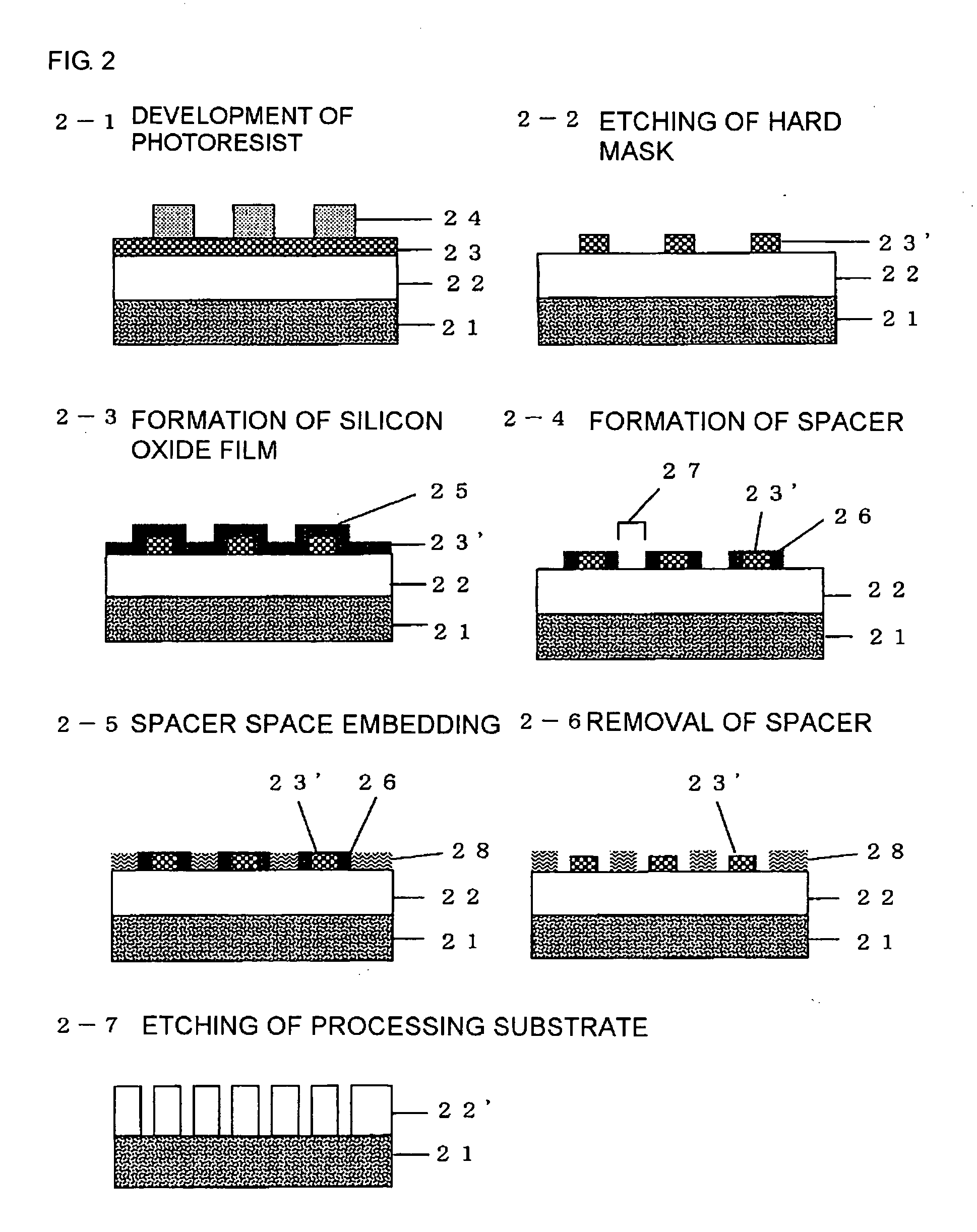
The present invention provides a patterning process that avoids deformation of the photoresist pattern and an increase in LWR (Linewidth roughness) when a silicon oxide film is formed on the photoresist pattern sidewall. This is achieved by using a photoresist pattern with a high film strength, and forming a spacer on the photoresist pattern sidewall using a CVD or ALD method. The invention also provides a method for forming a silicon oxide film at a temperature equal to or lower than the glass transition temperature of the base polymer in the photoresist film composition, and using a chemically amplified positive resist composition. Additionally, the invention provides a method for improving the dimensional controllability in etching of the processing substrate by using an underlayer film having a high carbon density as a mask, and an anti-reflection film formed of a hydrocarbon material between the carbon film and the photoresist film.

Problems solved by technology

As mentioned above, in a sidewall spacer method in which a silicon oxide film is formed as a spacer on a photoresist pattern sidewall and an underlayer is processed based on this spacer, when the oxide film is formed directly on the photoresist pattern, there occurred problems such as a deformation of the photoresist pattern thereby causing problems such as contraction of a dimension of the photoresist pattern and an increase in LWR.

Method used


Image

  • Patterning process
  • Patterning process
  • Patterning process

Examples


example

[0109]Hereinafter, the present invention will be described specifically by Examples and Comparative Examples, but the present invention is not restricted by Examples and the like described hereinafter. Here, a weight-average molecular weight is an equivalent weight-average molecular weight relative to polystyrene measured by GPC.

Synthesis Examples of Base Polymers

[0110]A base polymer added in a photoresist film composition was obtained as following; each monomer as shown below was combined and copolymerized in tetrahydrofurane as a solvent, and a resulting product was crystallized out in methanol, washed repeatedly with hexane, isolated, and dried to obtain a copolymer (base polymer) with a composition as shown below (polymers 1 to 9 and comparative polymers 1 and 2). Composition of an obtained base polymer was determined by 1H-NMR, and a molecular weight (weight average molecular weight) and a dispersivity (molecular weight distribution) were obtained by a gel permeation chromatogr...


PUM

PropertyMeasurementUnit
Young's modulusaaaaaaaaaa
wavelengthaaaaaaaaaa

Abstract

There is disclosed a patterning process including steps of at least: forming a photoresist film on a substrate; exposing the photoresist film to a high energy beam; developing by using a developer; forming a photoresist pattern; and then forming a spacer on the photoresist pattern sidewall, thereby forming a pattern on the substrate, a patterning process, wherein at least the photoresist pattern having the hardness of 0.4 GPa or more or the Young's modulus of 9.2 GPa or more as a film strength is formed, and a pattern is formed on the substrate by forming a silicon oxide film as the spacer on the photoresist pattern sidewall. There can be provided a patterning process without causing a deformation of a resist pattern and an increase in LWR at the time of forming a silicon oxide film on a photoresist pattern.

Description

BACKGROUND OF THE INVENTIONField of the Invention[0001]The present invention relates to a patterning process using a sidewall spacer method.[0002]In recent years, as LSI progresses toward higher integration and further acceleration in speed, miniaturization of a pattern rule is required. In the light-exposure used as a general technology nowadays, resolution inherent to wavelength of a light source is approaching to its limit. In 1980s, a g-line (436 nm) or an i-line (365 nm) of a mercury lamp was used as an exposure light. As a mean for further miniaturization, shifting to a shorter wavelength of an exposing light was assumed to be effective. As a result, in a mass production process after DRAM (Dynamic Random Access Memory) with 64-megabits (0.25 μm or less of a processing dimension) in 1990s, a KrF excimer laser (248 nm), a shorter wavelength than an i-beam (365 nm), was used in place of an i-line as an exposure light source.[0003]However, in production of DRAM with an integratio...

Claims


Application Information

Patent Timeline
Patent Type & Authority Applications(United States)
IPC IPC(8): G03F7/20
CPCH01L21/0275H01L21/0337H01L21/0332G03F7/20H01L21/027
Inventor HATAKEYAMA, JUNKATAYAMA, KAZUHIROKAWAI, YOSHIO
Owner SHIN ETSU CHEM IND CO LTD
Learn More