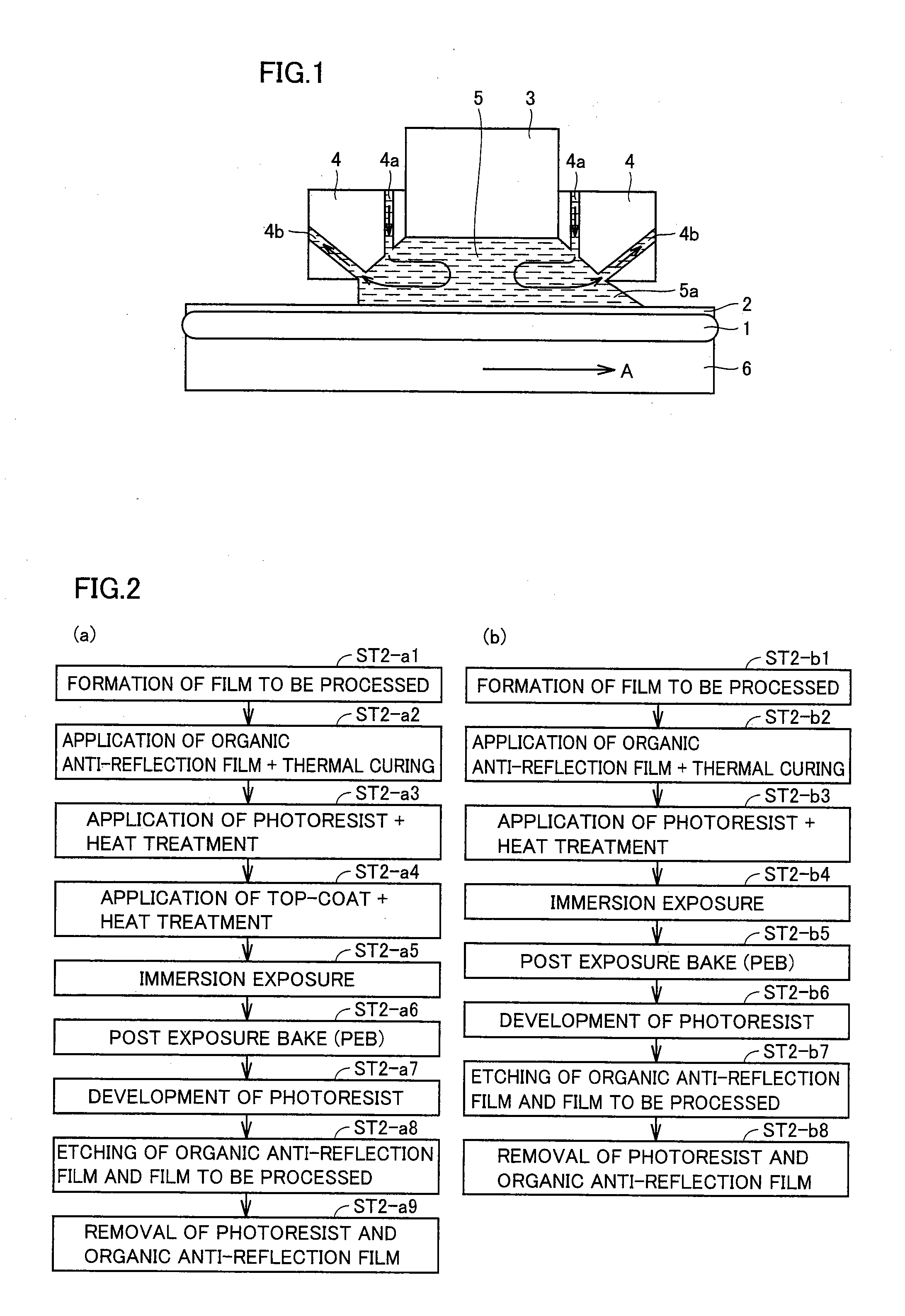
Developing method for immersion lithography, solvent used for the developing method and electronic device using the developing method
a technology of developing method and developing method, which is applied in the direction of photosensitive material processing, photomechanical equipment, instruments, etc., can solve the problems of high material cost and difficulty in achieving repellency sufficient for high-speed scanning, defects caused by immersion increase, and problems marked increase, so as to achieve low solubility and improve the performance of resist surface cleaning
- Summary
- Abstract
- Description
- Claims
- Application Information
AI Technical Summary
Benefits of technology
Problems solved by technology
Method used
Image


Examples
example 1
[0078]FIG. 9 shows a process flow of steps for manufacturing an electronic device, including the development method for immersion lithography as Example 1, and FIG. 10 includes schematic illustrations of each of the steps. In Example 1, the step of dissolving and removing is performed before the step of development with alkali immersion.
[0079]As shown in FIG. 10(a), a film 8 to be processed was formed on a substrate 7 (ST5-1 of FIG. 9), an organic anti-reflection film 9 (film thickness: 78 nm) was applied on film 8 to be processed, and heat treatment (hereinafter also referred to as baking) was performed at 205° C. for 90 seconds (ST5-2 of FIG. 9, FIG. 10(b)). Thereafter, commercially available top-coatless resists A to C containing surface segregation agents (water repellent agents) having different characteristics listed in Table 1 were each applied by spin-coating under conditions shown in Table 1, and thereafter baked to form photoresist film 10 (ST5-3 of FIG. 9 and FIG. 10(c))....
example 2
[0091]FIG. 11 shows a process flow showing steps of manufacturing an electronic device, including the developing method for immersion lithography in accordance with Example 2. FIG. 12 includes schematic illustrations of respective steps. In Example 2, the dissolving and removing step was conducted simultaneously with the developing step of alkali immersion.
[0092]On a substrate 7 having a film 8 to be processed, an organic anti-reflection film 9 and photoresist film 10 were formed by the method used in Example 1. Substrate 7 was subjected to exposure process by immersion exposure through mask 11, and post exposure bake was conducted at 110° C. for 60 seconds (ST7-1 to ST7-5 of FIG. 11, FIGS. 12(a) to (e)).
[0093]Thereafter, using a top-coatless resist developer prepared by mixing 2.38% solution of tetramethyl ammonium hydroxide (TMAH), isobutanol and ethanol at the volume ratio of 2:1:1, the surface segregation agent existing at the surface layer portion of photoresist film 10 was sel...
example 3
[0096]FIG. 13 shows a process flow showing steps of manufacturing an electronic device, including the developing method for immersion lithography in accordance with Example 3. FIG. 14 includes schematic illustrations of respective steps. In Example 3, the dissolving and removing step was conducted after the developing step by alkali immersion.
[0097]On a substrate 7 having a film 8 to be processed, an organic anti-reflection film 9 and photoresist film 10 were formed by the method used in Example 1. Substrate 7 was subjected to exposure process by immersion exposure through mask 11, and post exposure bake was conducted at 80 to 120° C. for 60 seconds (ST9-1 to ST9-5 of FIG. 13, FIGS. 14(a) to (e)).
[0098]Thereafter, development process was conducted using 2.38% solution of tetramethyl ammonium hydroxide (TMAH). Next, using Solvents 1 to 7 (dissolving and removing solutions) shown in Table 2, the surface segregation agents existing at the upper layer portion of photoresist film 10 were...
PUM
| Property | Measurement | Unit |
|---|---|---|
| surface | aaaaa | aaaaa |
| dissolving | aaaaa | aaaaa |
| surface tension | aaaaa | aaaaa |
Abstract
Description
Claims
Application Information
 - R&D
- Intellectual Property
- Life Sciences
- Materials
- Tech Scout
- Unparalleled Data Quality
- Higher Quality Content
- 60% Fewer Hallucinations
Browse by: Latest US Patents, China's latest patents, Technical Efficacy Thesaurus, Application Domain, Technology Topic, Popular Technical Reports.
© 2025 PatSnap. All rights reserved.Legal|Privacy policy|Modern Slavery Act Transparency Statement|Sitemap|About US| Contact US: help@patsnap.com