Bonded intermediate substrate and method of making same
- Summary
- Abstract
- Description
- Claims
- Application Information
AI Technical Summary
Benefits of technology
Problems solved by technology
Method used
Image
Examples
first embodiment
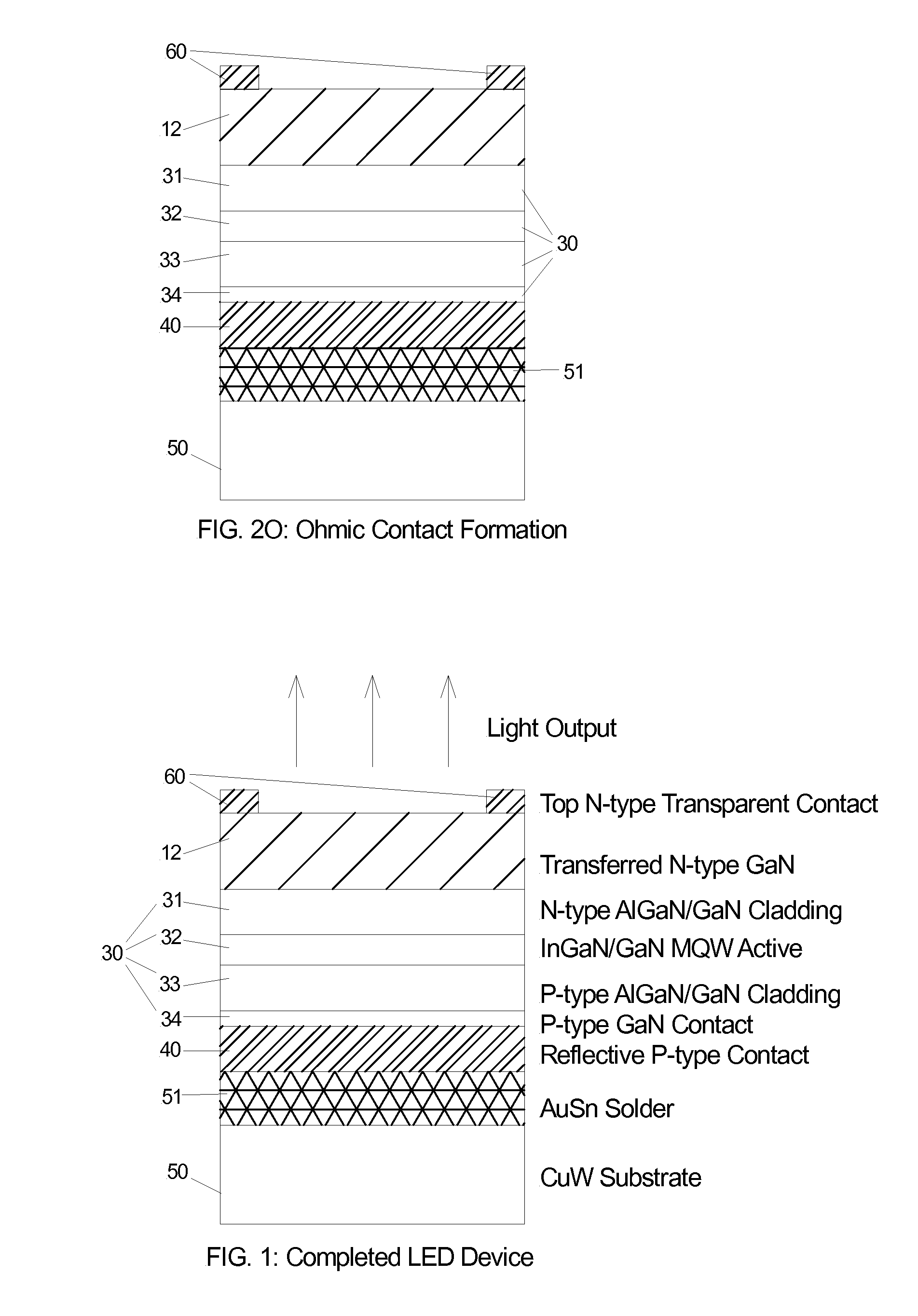
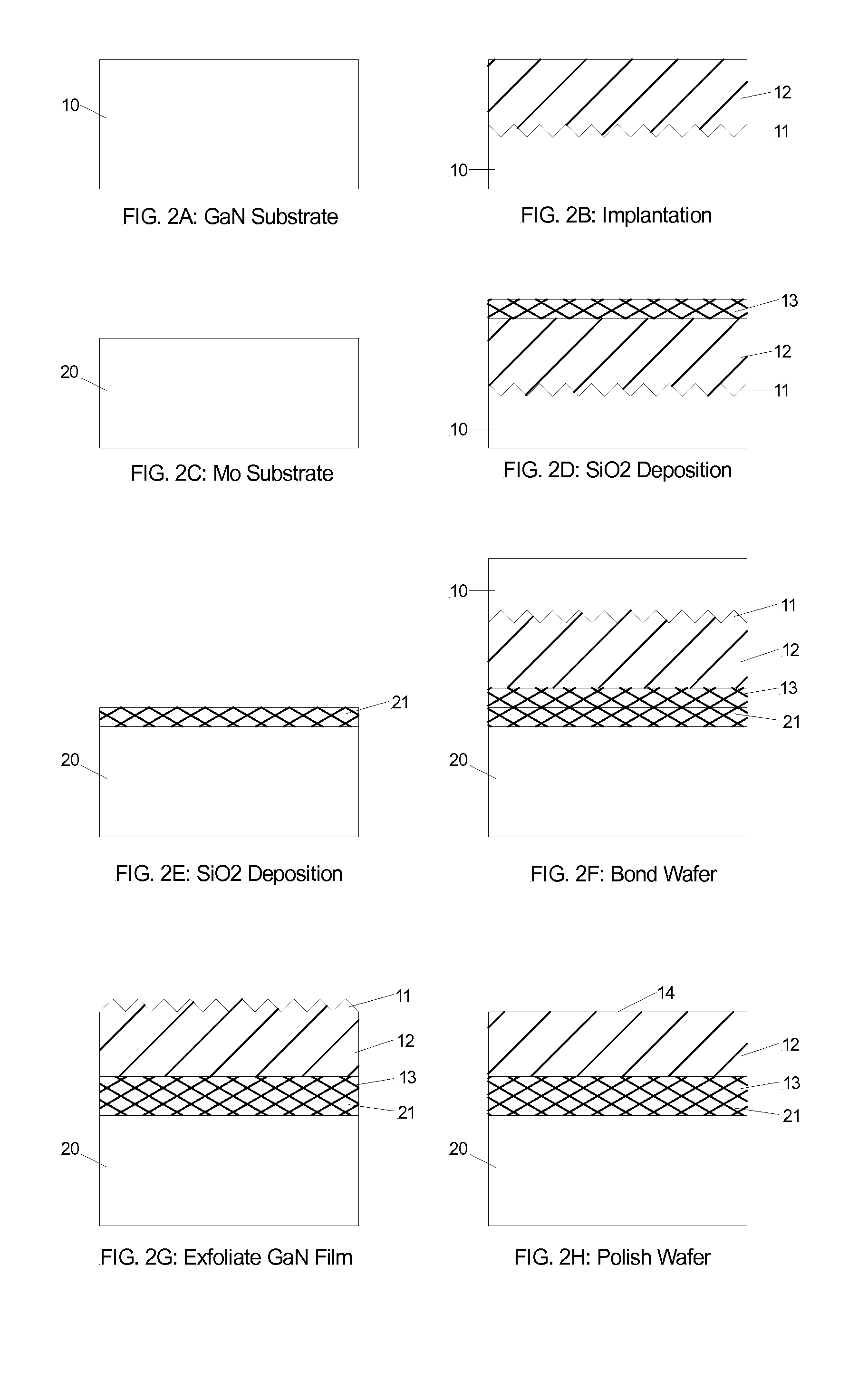
[0028]Detailed processing techniques and structures in accordance with embodiments of the present invention are illustrated in FIGS. 2A-2O, 3A-3C, 5A, and 5B. FIGS. 2A-2O illustrate a method of the In FIG. 2A, a source (also known as “donor”) semiconductor substrate or wafer 10 is preferably high-quality low-defect-density freestanding commercial GaN substrate, where dislocation-defect density is less than 108 / cm2. Other preferred candidates for source wafer 10 comprise one or more layers of GaN or AlzGa1-zN materials grown homo-epitaxially on high-quality low-defect-density freestanding commercial GaN or AlN substrates, where z is in the range of 0 to 1. Other possible candidates for source wafer 10 comprise one or more layers of GaN or AlzGa1-zN materials grown heteroepitaxially on sapphire or SiC substrates. These hetero-epitaxially grown materials have higher dislocation-defect density, typically higher than 108 / cm2.
[0029]Alternatively, as will be described with respect to the ...
second embodiment
[0174]In an alternative second embodiment, rather than bonding a III-nitride semiconductor source wafer 10 to the handle substrate and then exfoliating a thin III-nitride semiconductor layer 12 from the semiconductor source wafer, a single-crystalline material which supports epitaxial growth of III-nitride semiconductor layers is bonded to the handle substrate. This single-crystal material comprises sapphire, silicon carbide or any other suitable material which supports epitaxial growth of III-nitride semiconductor layers such as GaN, InGaN, AlGaN, etc. Thus, the GaN substrate 10 shown in FIG. 2A is substituted with a single-crystalline material comprising sapphire, SiC, or other ceramic materials.
[0175]A thin transferred layer 12 from a single-crystal material such as sapphire, may be formed on the handle substrate using an ion implantation-induced exfoliation from a bulk substrate, as shown in FIGS. 2A-2H, or using a substrate bond and etch-back process (i.e., etching and / or polis...
third embodiment
[0181]In a third embodiment, an epitaxially-grown layer on a source wafer 10 can be bonded to the handle substrate 20. Preferably, the epitaxially-grown layer on a source wafer 10 comprises a film of AlGaN grown epitaxially on a sapphire or SiC substrate, using techniques known in the art such as HVPE, MOCVD or MBE. In this embodiment the GaN source wafer 10 in FIG. 2A is substituted with an epitaxially-grown layer on a substrate comprising an AlxGa1-xN layer on a SiC or sapphire substrate, such that a thin layer of the AlxGa1-xN layer, where 0≦x≦1, is bonded and transferred to the handle substrate.
[0182]A thin transferred layer 12 of the epitaxially-grown AlGaN film may be formed on the handle substrate 20 using exfoliation or a substrate bond and etch-back process. Further processing of this third embodiment is similar to the process steps already shown in the Figures and described above.
PUM
 Abstract
Description
Claims
Application Information
 - R&D
- Intellectual Property
- Life Sciences
- Materials
- Tech Scout
- Unparalleled Data Quality
- Higher Quality Content
- 60% Fewer Hallucinations
Browse by: Latest US Patents, China's latest patents, Technical Efficacy Thesaurus, Application Domain, Technology Topic, Popular Technical Reports.
© 2025 PatSnap. All rights reserved.Legal|Privacy policy|Modern Slavery Act Transparency Statement|Sitemap|About US| Contact US: help@patsnap.com


