Surface emitting laser
- Summary
- Abstract
- Description
- Claims
- Application Information
AI Technical Summary
Benefits of technology
Problems solved by technology
Method used
Image
Examples
exemplary embodiment 1
[0062]In Exemplary embodiment 1, a photonic-crystal surface emitting laser to which the present invention is applied will be described.
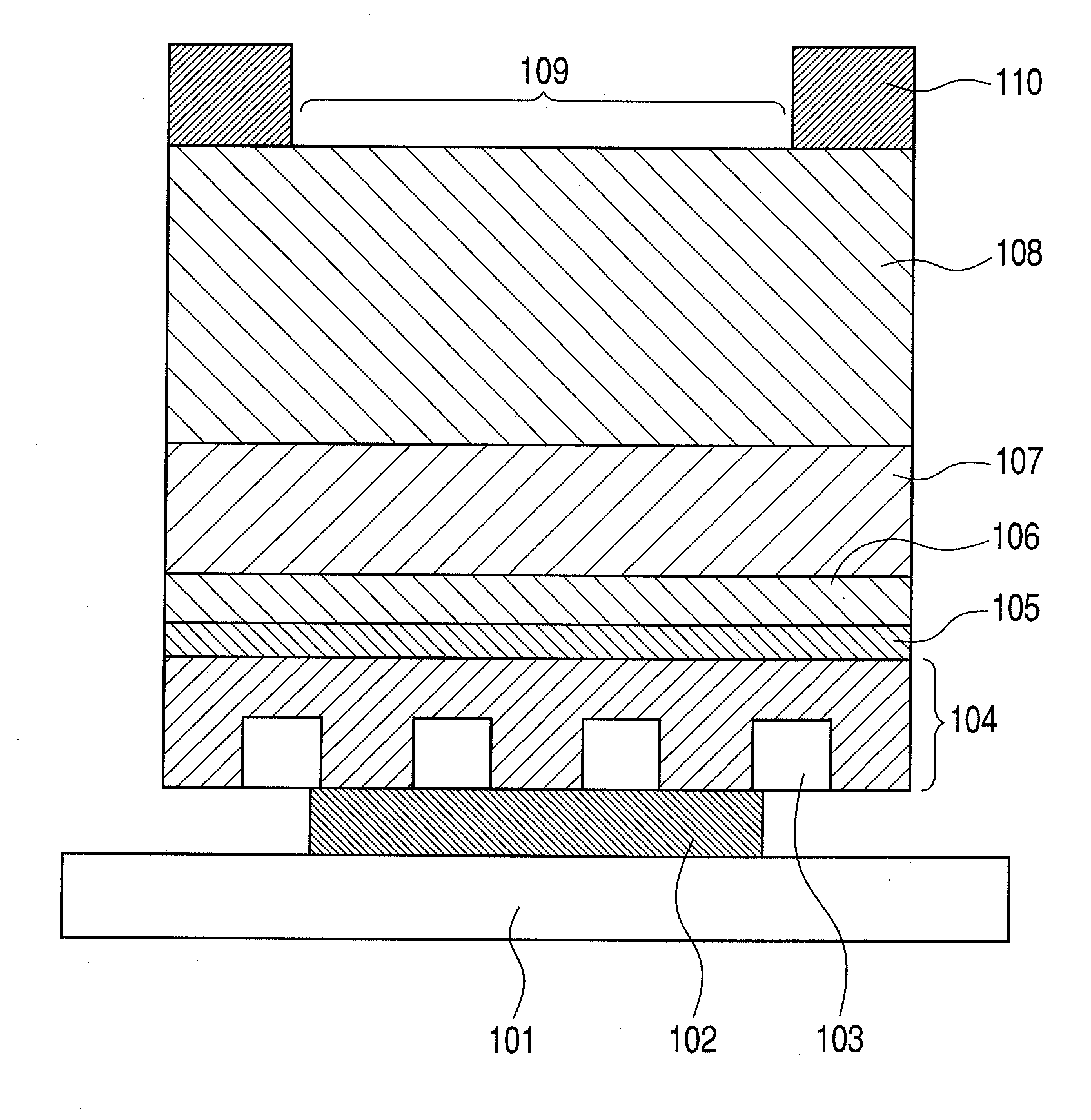
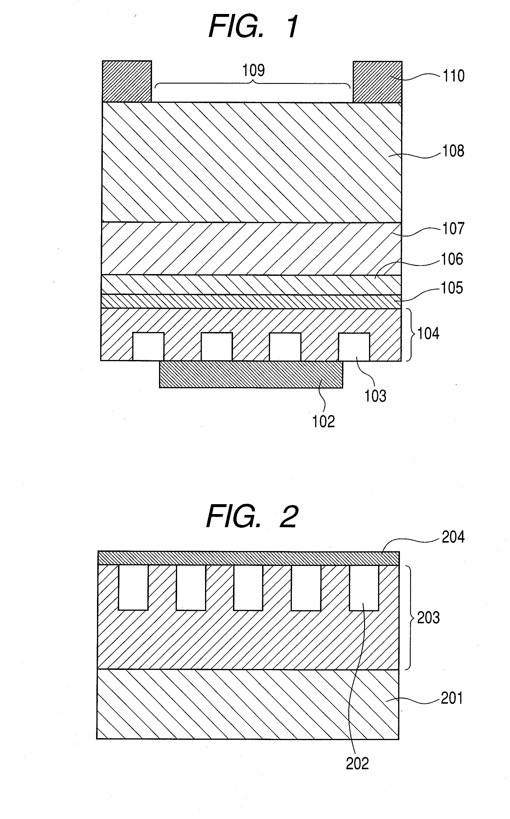
[0063]FIG. 4 illustrates a schematic sectional view for describing a structure of a photonic-crystal surface emitting laser to which the present invention is applied.
[0064]In FIG. 4, the same element as that illustrated in FIG. 1 is designated by the same reference numeral. An SiC substrate 101 has an electrode pattern on its surface.
[0065]The surface emitting laser of the present embodiment is constituted by a plurality of semiconductor layers including a photonic crystal structure 103 laminated on a GaN substrate 108, and emits a laser beam having a wavelength λ from the rear face side with respect to the laminated face of the semiconductor layers.
[0066]Specifically, a p-type electrode 102 is formed so as to contact with a p-GaN layer 104 (photonic crystal layer) in which the photonic crystal structure 103 has been produced up to the middle of the ...
exemplary embodiment 2
[0088]In Exemplary embodiment 2, a structure example including a multilayer reflector in the photonic crystal layer will now be described.
[0089]In the present exemplary embodiment, the multilayer reflector formed of semiconductors is provided in the photonic crystal layer, and accordingly can enhance the light extraction efficiency.
[0090]FIG. 6 illustrates a schematic sectional view for describing a structure of a surface emitting laser in the present exemplary embodiment.
[0091]In FIG. 6, the same element as that illustrated in FIG. 1 is designated by the same reference numeral. The structure of the present exemplary embodiment has a semiconductor DBR 605 formed of laminated mirrors of a pair of two types of semiconductor layers 602 and 603 having mutually different refractive indices in the photonic crystal layer, which is a different point.
[0092]In the present exemplary embodiment, the first semiconductor layer 602 of the semiconductor DBR 605 is made from the same material as tha...
exemplary embodiment 3
[0098]In Exemplary embodiment 3, a structure example will now be described in which a multilayer reflector formed of semiconductors is provided in a region on the laser beam emission side, which region is farther than the p-type semiconductor layer in the above described laminated structure.
[0099]A photonic-crystal surface emitting laser in the present exemplary embodiment is structured so that a DBR is formed in the n-side, and so that the Q-value and extraction efficiency can be controlled.
[0100]FIG. 7 illustrates a schematic sectional view for describing a structure of a photonic-crystal surface emitting laser according to the present exemplary embodiment.
[0101]In FIG. 7, the same element as that illustrated in FIG. 1 is designated by the same reference numeral.
[0102]The present exemplary embodiment has basically the same structure as in Exemplary embodiment 1, but is different from Exemplary embodiment 1 in that a DBR 703 is provided on an n-cladding layer.
[0103]In the present e...
PUM
 Abstract
Description
Claims
Application Information
 - R&D Engineer
- R&D Manager
- IP Professional
- Industry Leading Data Capabilities
- Powerful AI technology
- Patent DNA Extraction
Browse by: Latest US Patents, China's latest patents, Technical Efficacy Thesaurus, Application Domain, Technology Topic, Popular Technical Reports.
© 2024 PatSnap. All rights reserved.Legal|Privacy policy|Modern Slavery Act Transparency Statement|Sitemap|About US| Contact US: help@patsnap.com


