
Method of forming measuring targets for measuring dimensions of substrate in substrate manufacturing process

a technology of measuring targets and substrates, applied in the direction of instruments, photomechanical equipment, originals for photomechanical treatment, etc., can solve the problems of process yield and process accuracy reduction, and achieve the effect of not increasing the fabrication cost of the substrate and improving process alignmen

Active Publication Date: 2009-10-15
ASE ELECTRONICS
View PDF3 Cites 0 Cited by
  • Summary
  • Abstract
  • Description
  • Claims
  • Application Information

AI Technical Summary

Benefits of technology

[0006]Accordingly, the present invention is directed to a method for instantly measuring the dimensions of a substrate during a substrate manufacturing process, wherein the accuracy in process alignment is improved and accordingly the process yield is increased.
[0021]As described above, in the present invention, measuring targets for measuring the dimensions of a substrate are formed during a substrate manufacturing process so that the dimensions of the substrate can be instantly measured during the fabricating process thereof and accordingly the accuracy in process alignment can be improved. Moreover, according to the present invention, no additional step is to be executed in the original substrate manufacturing process. Thereby, the fabrication cost of the substrate is not increased.

Problems solved by technology

However, during the fabricating process of such a substrate, the dimensions of the base layer, the dielectric layers, or a solder resist (SR) layer may be changed by heat or other factors so that the accuracy thereof may be reduced and accordingly the process yield may be affected.

Method used


Image

  • Method of forming measuring targets for measuring dimensions of substrate in substrate manufacturing process
  • Method of forming measuring targets for measuring dimensions of substrate in substrate manufacturing process
  • Method of forming measuring targets for measuring dimensions of substrate in substrate manufacturing process

Examples


Embodiment Construction

[0025]Reference will now be made in detail to the present preferred embodiments of the invention, examples of which are illustrated in the accompanying drawings. Wherever possible, the same reference numbers are used in the drawings and the description to refer to the same or like parts.

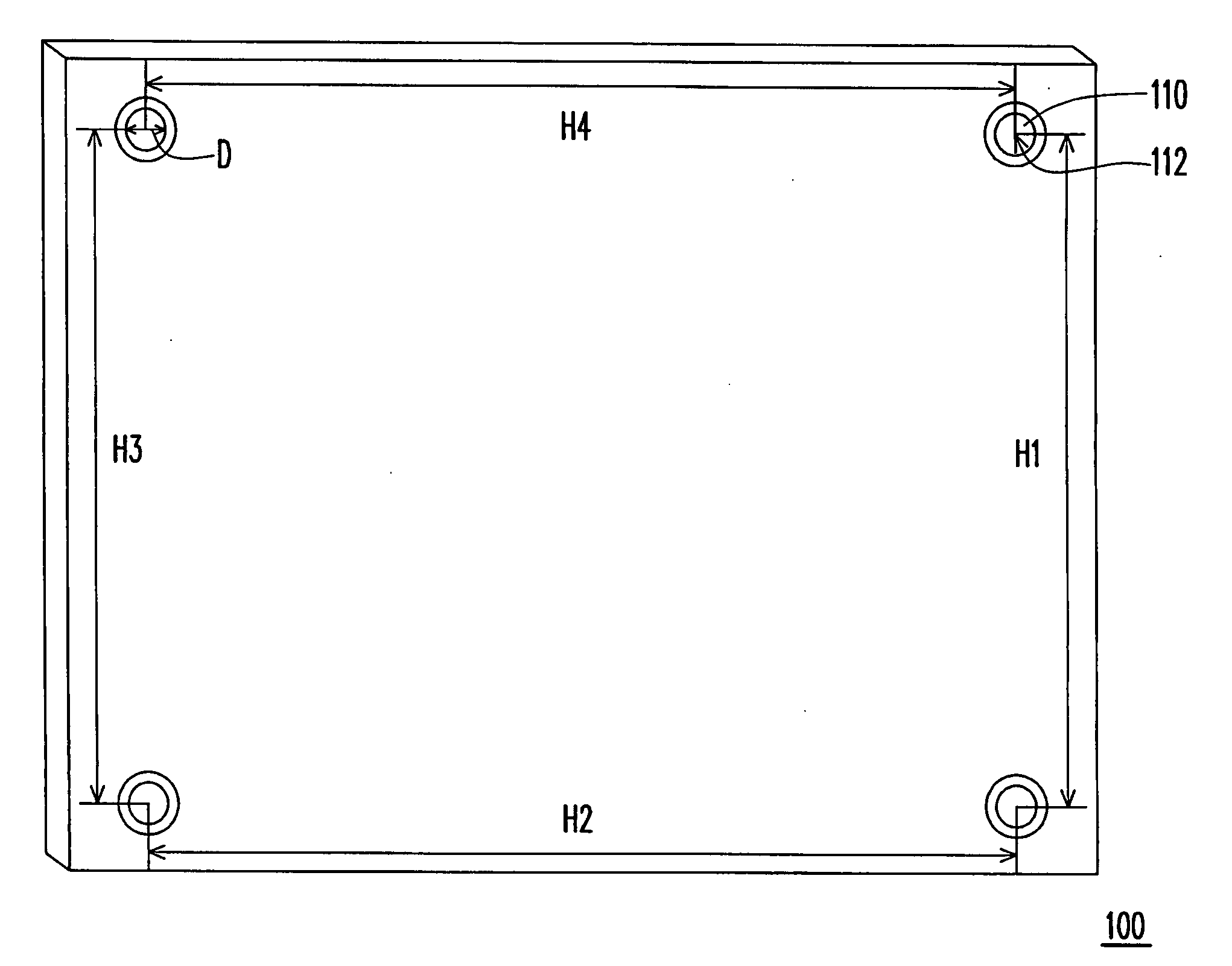
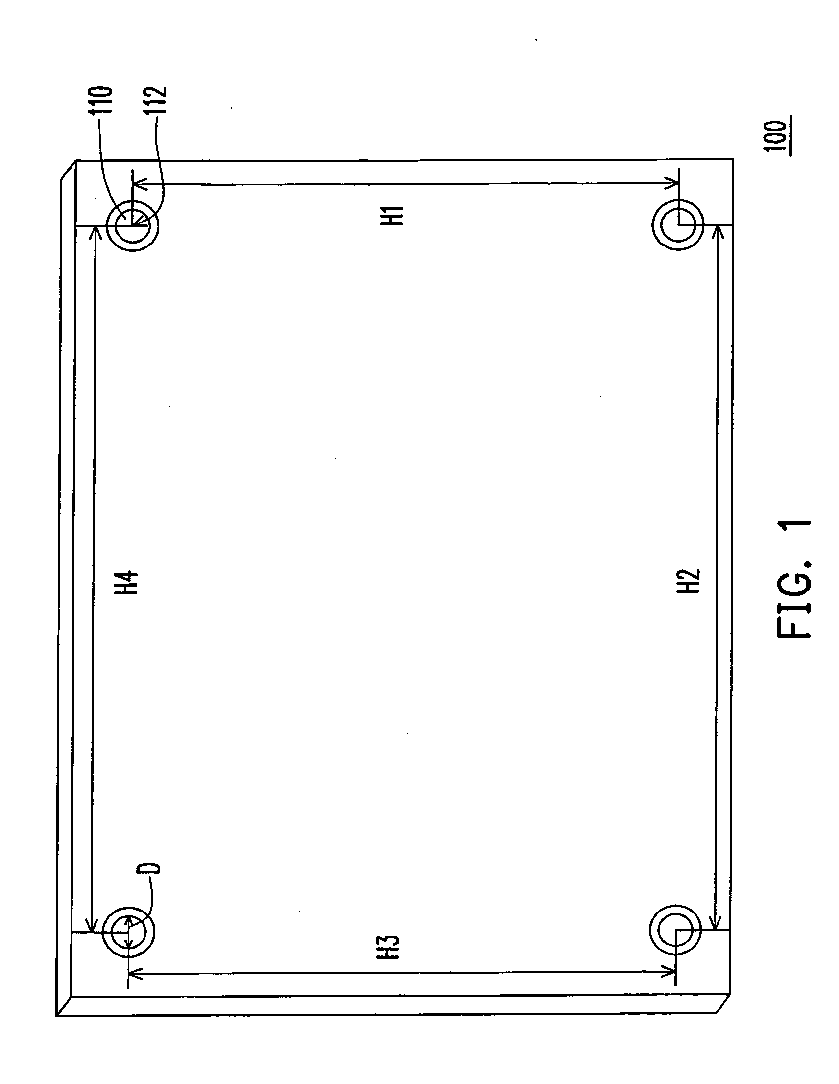
[0026]FIG. 1 illustrates a method for measuring the dimensions of a substrate by using measuring targets on the substrate according to an embodiment of the present invention.

[0027]Referring to FIG. 1, in the present embodiment, the substrate 100 has a plurality of measuring targets 110, and the measuring targets 110 can be disposed at any suitable position on the substrate 100. In the present embodiment, the measuring targets 110 may be formed at four corners of the substrate 100, wherein the dimensions of the substrate 100 can be instantly measured by using the measuring targets 110 during the fabricating process of the substrate 100 and accordingly the accuracy in process alignment can be increased...


PUM


Abstract

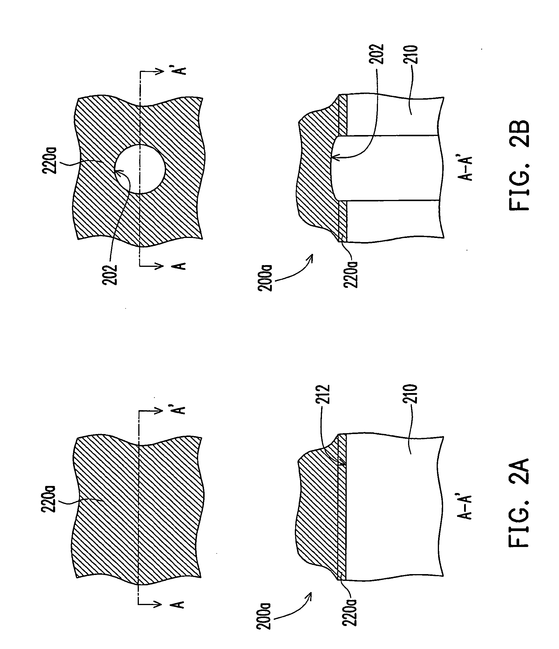
A method of forming measuring targets for measuring the dimensions of a substrate during a substrate manufacturing process is provided. First, a board having a base layer and a conductive layer is provided, wherein the conductive layer is disposed on a surface of the base layer. Then, at least one through hole is formed in the board as a measuring target for measuring the dimensions of the substrate. Next, a plated via is formed in the through hole as another measuring target for measuring the dimensions of the substrate. Thereafter, a patterned dielectric layer is formed on the board to expose the plated via as a next measuring target for measuring the dimensions of the substrate. In the present invention, measuring targets are formed during a substrate manufacturing process and the dimensions of the substrate are measured instantly. The accuracy in process alignment is improved without increasing the fabrication cost.

Description

CROSS-REFERENCE TO RELATED APPLICATION[0001]This application claims the priority benefit of Taiwan application serial no. 97113049, filed on Apr. 10, 2008. The entirety of the above-mentioned patent application is hereby incorporated by reference herein and made a part of this specification.BACKGROUND OF THE INVENTION[0002]1. Field of the Invention[0003]The present invention generally relates to a method of forming measuring targets for measuring the dimensions of a substrate, in particular, to a method of forming measuring targets for measuring the dimensions of a substrate in a substrate manufacturing process.[0004]2. Description of Related Art[0005]In recent years, the designs of both electronic products and the substrates adopted therein are going towards lightness, slimness, shortness, smallness, multifunctionality, and especially, high circuit density. In an existing method for fabricating a substrate of high circuit density, a hard base layer is provided as the core and circu...

Claims


Application Information

Patent Timeline
IPC IPC(8): G03F7/20
CPCH05K1/0269H05K1/116H05K3/427H05K2201/0989H05K3/4679H05K2201/09536H05K2201/0959H05K3/4602
Inventor FENG, HSIANG-MING
Owner ASE ELECTRONICS
Learn More