Surface shape measuring apparatus, exposure apparatus, and device manufacturing method

a technology of surface shape and measurement apparatus, applied in the direction of measurement devices, instruments, printing, etc., can solve the problems of non-negligible measurement errors of surface position detecting units, asymmetric reflection light, and generation of measurement errors, so as to achieve high-accuracy measurement of surface shapes

Inactive Publication Date: 2009-09-03
CANON KK
View PDF12 Cites 14 Cited by
  • Summary
  • Abstract
  • Description
  • Claims
  • Application Information

AI Technical Summary

Benefits of technology

[0017]According to an aspect of the present invention, a surface shape measuring apparatus can high-accurately measure a surface shape without being affected by reflectance distribution of a substrate and interference caused by a thin film.
[0019]With the surface shape measuring apparatus according to an aspect of the present invention, errors generated in the optical measurement can be reduced by suppressing the influence of the reflected light from the rear surface of a resist (film) based on properties that the phase of the p-polarized light is changed when the incident angle is larger than the Brewster's angle. Therefore, a surface shape measuring apparatus capable of accurately measuring the front surface position of a film, such as a resist is provided. Further, an exposure apparatus is provided which can realize high focus accuracy with respect to a small focal depth and which can increase yields.

Problems solved by technology

In particular, measurement errors of the surface position detecting unit have become non-negligible even when the measurement errors are caused by an influence of a pattern on the wafer and a variation in thickness of a resist coated on the wafer.
Thus, among the reflected lights detected by the surface position detecting unit, the reflected light from the rear surface of the resist is changed in reflection angle and reflection intensity, and a waveform obtained by detecting such reflected light becomes asymmetric and measurement errors are generated.
In other words, the barycenter of the reflected light is shifted from a predetermined position and measurement errors are generated.
Accordingly, the waveform of a signal detected by receiving the reflected light becomes asymmetrical and the contrast of the detected signal waveform deteriorates significantly, thus causing a difficulty in accurately measuring the wafer surface position.
Such a difficulty results in a large defocus and a chip failure.
In some cases, therefore, it is difficult to accurately detect a position on the wafer surface by receiving the reflected light.
This leads to a difficulty in accurately detecting height information of the resist front surface by using only the reflected light from the front surface of the resist.
However, when the substrate is made of Al or Cu and has high reflectance, the rear surface of the resist (i.e., the resist / substrate interface) has high reflectance to such an extent that the influence of the reflected light from the rear surface of the resist cannot be sufficiently suppressed even when the incident angle of the light upon the substrate is set to a large value.
Accordingly, errors are generated in a value resulting from measuring the resist front surface.
Further, when a gas gauge sensor is used as described in PCT Application Domestic Laid-Open No. 2006-514744, specific problems arise in that fine particles mixed in gas are also sprayed onto the wafer, and that the gas gauge sensor cannot be used in an exposure apparatus operating in vacuum, e.g., an EUV (Extreme Ultraviolet) exposure apparatus using an extreme ultraviolet light, because a degree of vacuum deteriorates with the sprayed gas.

Method used


Image

  • Surface shape measuring apparatus, exposure apparatus, and device manufacturing method
  • Surface shape measuring apparatus, exposure apparatus, and device manufacturing method
  • Surface shape measuring apparatus, exposure apparatus, and device manufacturing method

Examples


Embodiment Construction

[0045]Exemplary embodiments of the present invention will be described below with reference to the accompanying drawings. Note that, throughout the drawings, the same components are denoted by the same reference numerals, and redundant description is omitted.

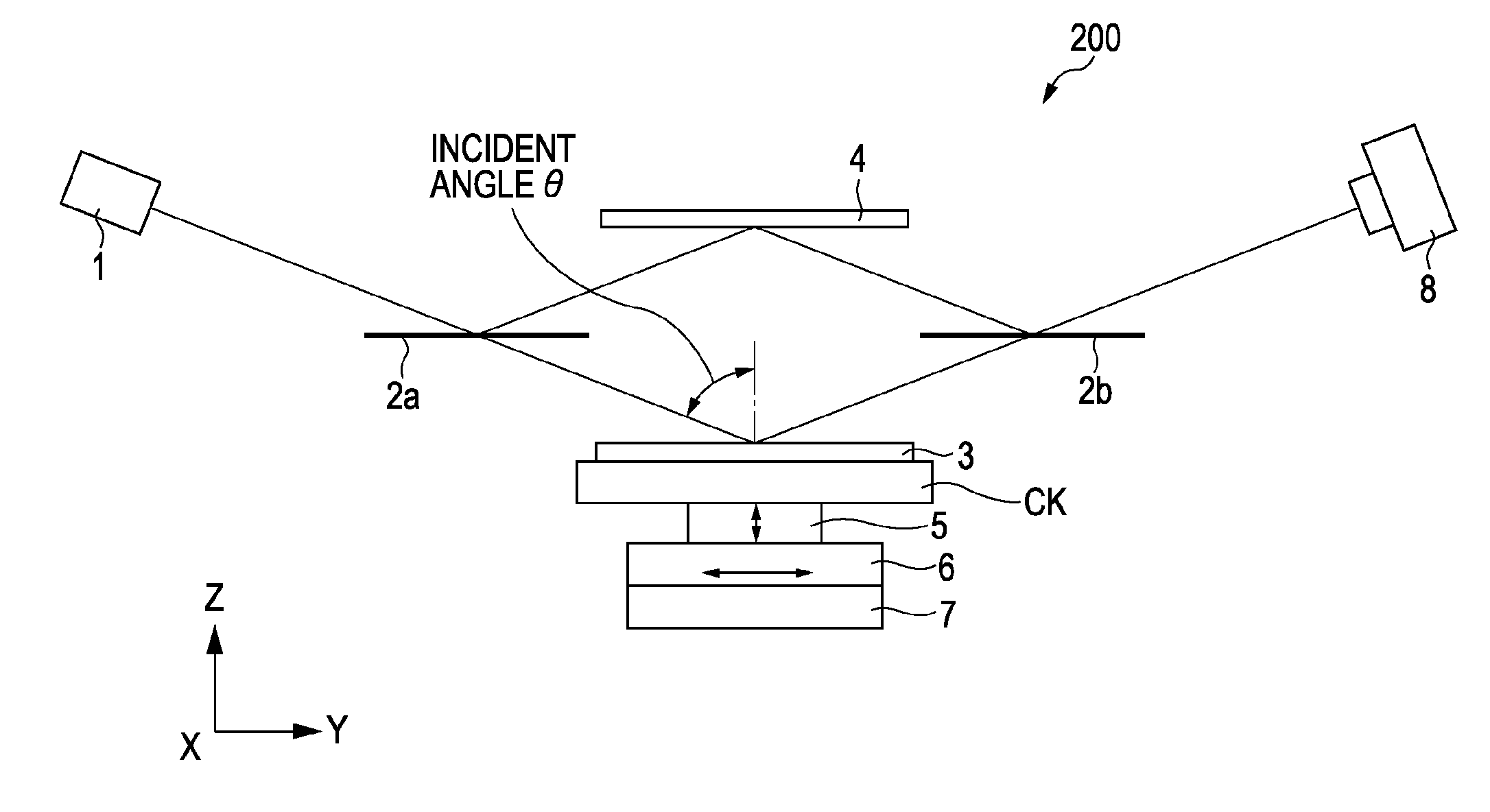
[0046]FIG. 1 is a block diagram of a surface shape measuring apparatus 200 according to a first exemplary embodiment of the present invention. The surface shape measuring apparatus 200 is an apparatus configured to detect the surface position of a film on a substrate 3, i.e., a measurement target having the film on its surface, in the height direction (Z-direction). More specifically, the surface shape measuring apparatus 200 includes a light source 1 provided as a halogen lamp or an LED (including the so-called white LED) each emitting wide-band light, a beam splitter (BS) 2a arranged to branch the light, and a substrate chuck CK arranged to hold the measurement target 3. Further, the surface shape measuring apparatus 200 inclu...


PUM


Abstract

A surface shape measuring apparatus includes an illumination system and a light receiving system. The illumination system splits wide-band light from a light source into measurement light and reference light, illuminates the measurement light to obliquely enter a surface of the film, and illuminates the reference light to obliquely enter a reference mirror. The light receiving system combines the measurement light reflected by the surface of the film and the reference light reflected by the reference mirror with each other and introduces the combined light to a photoelectric conversion element. An incident angle of the measurement light upon the surface of the film and an incident angle of the reference light upon the reference mirror are each larger than the Brewster's angle. S-polarized light and p-polarized light included in the measurement light entering a surface of the substrate have equal intensity on the photoelectric conversion element.

Description

BACKGROUND OF THE INVENTION[0001]1. Field of the Invention[0002]The present invention relates to surface shape measuring apparatuses and exposure apparatuses.[0003]2. Description of the Related Art[0004]The related art regarding a surface shape measuring apparatus and an exposure apparatus employing the former is described in connection with a semiconductor exposure apparatus which needs high accuracy in surface shape measurement.[0005]When a microstructural semiconductor device or liquid crystal display device, such as a semiconductor memory or a logical circuit, is manufactured by using photolithography (printing) techniques, a projection exposure apparatus is used to project and transfer a circuit pattern, which is drawn on a reticle (mask), onto a wafer, etc. through a projection optical system.[0006]In the projection exposure apparatus, a higher packing density of a semiconductor device causes a demand for projecting the circuit pattern on the reticle to the wafer for exposure ...

Claims


Application Information

Patent Timeline
Patent Type & Authority Applications(United States)
IPC IPC(8): G01B9/02
CPCG01B11/0608G01B11/2441G03F9/7026G01B9/02072G01B9/0209G01B9/02063G01B2290/70G03F9/7049G03F7/70516G03F7/7055
Inventor YAMAGUCHI, WATARUMATSUMOTO, TAKAHIROINA, HIDEKI
Owner CANON KK
Why Eureka
Try Eureka