AlInGaN LIGHT-EMITTING DEVICE

a technology of light-emitting devices and laser diodes, which is applied in the direction of lasers, semiconductor lasers, solid-state devices, etc., can solve the problems of significant lower threshold currents of laser diodes, and achieve the effect of improving the temperature stability of output and improving the wavelength of light-emitting diodes

Inactive Publication Date: 2009-07-16
SHARP KK
View PDF0 Cites 33 Cited by
  • Summary
  • Abstract
  • Description
  • Claims
  • Application Information

AI Technical Summary

Benefits of technology

[0012]It has been found that providing the AlGaN layer on the substrate side of an InGaN quantum dot or quantum wire active region provides a greater optical power output. This is believed to result from improved injection of carriers into the active region; that is, the AlxGa1-xN layer serves, in use, to promote the injection of carriers into the active region. The improvement in optical power output decreases as the separation between the AlxGa1-xN layer and the active region increases, so that the AlxGa1-xN layer is preferably close to the active region. It has been found that the separation between the AlxGa1-xN layer and the active region should be not more that 25 nm to obtain a significant increase in optical power output.
[0013]A difference between the lattice constant of the AlxGa1-xN layer and the lattice constant of the active region may be not more than 3%. This minimises the stress / strain introduced into the device, and so prevents any adverse effect on the device performance and / or lifetime. As explained above, the AlxGa1-xN layer is provided to increase the optical power output of the device by, it is believed, promoting injection of carriers into the active region—the AlxGa1-xN layer is not provided for strain compensation purposes.
[0014]The AlGaN layer may have a thickness greater than 5 nm, and it may have a thickness less than 50 nm. It has been found that this thickness range for the AlGaN layer provides significant improvement in the optical power output of the device.
[0016]The InGaN quantum dot layer or quantum wire layer, or the first grown InGaN quantum dot layer or quantum wire layer if the active region contains two or more quantum dot layers or quantum wire layers, may be directly on top of the AlGaN layer. Alternatively, there may be a (In)GaN layer between the AlGaN layer and the (first) InGaN quantum dot layer or quantum wire layer. Since the formation of quantum dots or quantum wires is dependant on the lattice parameter and the surface energy of the underlying layer, it may be advantageous to grow the first layer of quantum dots or quantum wires on a layer of the same composition as the barrier layer separating the multiple quantum dot layers or quantum wire layers. Therefore all quantum dot layers or quantum wire layers would be grown on identical underlying layers. This may maximise the uniformity of the quantum dot layers or quantum wire layers.
[0019]Use of a quantum dot active region also improves the temperature stability of the output from a light-emitting device.
[0020]FIG. 3b shows the improvement in temperature stability of the wavelength of a light emitting diode when a quantum dot active region is used (open circles) instead of a quantum well active region (filled circles).

Problems solved by technology

In addition the very narrow density of states obtainable with a quantum dot active region owing to the 3D confinement results in a narrow gain spectra leading to significantly lower threshold currents for laser diodes.

Method used


Image

  • AlInGaN LIGHT-EMITTING DEVICE
  • AlInGaN LIGHT-EMITTING DEVICE
  • AlInGaN LIGHT-EMITTING DEVICE

Examples


Embodiment Construction

[0028]In the following, preferred embodiments of the invention are described in more detail.

[0029]A light-emitting device of the present invention may be manufactured using any suitable growth technique such as molecular beam epitaxy (MBE) or metal-organic vapour phase epitaxy (MOVPE). The invention is not limited to any specific growth technique. Any source of active nitrogen may be used in fabricating the present invention; this includes, but is not limited to NH3 and a nitrogen plasma.

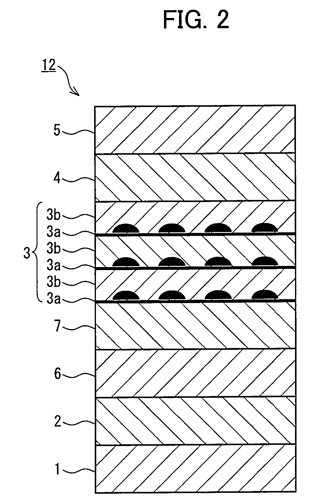
[0030]FIG. 2 is a schematic sectional view of a light-emitting device according to an embodiment of the invention. In this embodiment the light-emitting device is a light-emitting diode 12. The light-emitting device is fabricated in the (Al,Ga,In)N materials system.

[0031]The light emitting diode 12 of FIG. 2 comprises a substrate 1. The substrate may consist of any material with a suitable lattice parameter for growth of (Al,Ga,In)N. The substrate may comprise, but is not limited to, GaN, sapphire o...


PUM


Abstract

A semiconductor light-emitting device fabricated in the (Al,Ga,In)N materials system has an active region for light emission (3) comprising InGaN quantum dots or InGaN quantum wires. An AlGaN layer (6) is provided on a substrate side of the active region. This increases the optical output of the light-emitting device. This increased optical output is believed to result from the AlxGa1-xN layer serving, in use, to promote the injection of carriers into the active region.

Description

[0001]This Nonprovisional application claims priority under U.S.C. § 119(a) on Patent Application No. 0800742.9 filed in U.K. on Jan. 16, 2008, the entire contents of which are hereby incorporated by reference.FIELD OF THE INVENTION[0002]The invention relates to light emitting devices fabricated in the AlGaInN material system and, in particular, to such light-emitting devices having an active region that includes InGaN quantum dots or quantum wires.BACKGROUND OF THE INVENTION[0003]A semiconductor quantum dot is a volume of semiconductor material different from that of the surrounding matrix with a dimension of typically less than 50 nm in all directions. The small size results in the confinement of carriers (electrons or holes, or both electrons and holes), and therefore the presence of quantum size effects, in all three dimensions. The observation of individual quantum dots, and the behaviour due to the quantum confinement in all three dimensions (such as changes in the temperature...

Claims


Application Information

Patent Timeline
Patent Type & Authority Applications(United States)
IPC IPC(8): H01L33/00H01L33/08H01L33/32
CPCB82Y20/00H01L33/08H01L33/32H01S5/34333H01S5/341H01S5/3412H01S5/0213
Inventor SMITH, KATHERINE LOUISESENES, MATHIEU XAVIERSMEETON, TIM MICHAELHOOPER, STEWART EDWARD
Owner SHARP KK
Why Eureka
Try Eureka