
Low inductance, high rating capacitor devices

a capacitor and low inductance technology, applied in the field of low inductance and high rating capacitor devices, can solve the problems of generating unacceptable voltage spikes, needing to reduce inductance, and relatively large (i.e., high value or rating) capacitors, and achieve the effect of reducing the inductance of such multi-layer electronic components

Inactive Publication Date: 2009-06-11
AVX CORP
View PDF4 Cites 86 Cited by
  • Summary
  • Abstract
  • Description
  • Claims
  • Application Information

AI Technical Summary

Benefits of technology

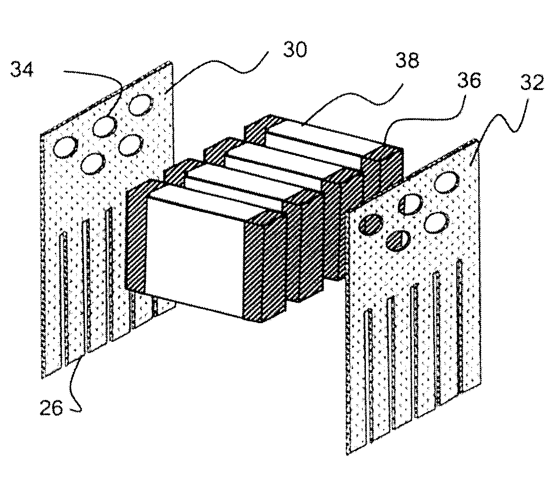
[0025]In the foregoing exemplary embodiment, preferably such pair of lead frame elements are respectively connected structurally and electrically with such first and second conductive termination layers, and configured so that such first and second electrode layers are in a vertical position relative to an associated circuit board, whereby a minimum current loop area is formed with such plurality of first and second electrode layers and the associated circuit of an associated circuit board, so as correspondingly reduce inductance of such multilayer electronic component.
[0032]Another present exemplary embodiment relates to a low inductance multilayer electronic capacitor, configured for mounting on a circuit board having an associated circuit, comprising a plurality of first electrode layers, with each first electrode layer comprising a first dielectric layer having first and second surfaces thereof and a first conductive layer covering a portion of such first surface of such first dielectric layer and extending to at least a portion of one edge of such first dielectric layer; a plurality of second electrode layers alternately stacked with such plurality of first electrode layers, with each second electrode layer comprising a second dielectric layer having first and second surfaces thereof and a second conductive layer covering a portion of such first surface of such second dielectric layer and extending to at least a portion of one edge of such second dielectric layer, the second conductive layer formed as a mirror image of the first conductive layer; a first conductive termination layer covering a portion of such at least one edge of such first electrode layer and electrically connecting such first conductive layer of each of such plurality of first electrode layers; a second conductive termination layer covering a portion of such at least one edge of such second electrode layer and electrically connecting such second conductive layer of each of such plurality of second electrode layers; and a pair of lead frame elements respectively connected structurally and electrically with such first and second conductive termination layers, and configured so that such first and second electrode layers are in a vertical position relative to an associated circuit board. Advantageously, with the foregoing exemplary arrangement, a minimum current loop area is formed with such plurality of first and second electrode layers and the associated circuit of an associated circuit board, so as correspondingly reduce inductance of such multilayer electronic capacitor.
[0038]Another present exemplary methodology for making a low inductance multilayer electronic capacitor, configured for mounting on a circuit board having an associated circuit, may comprise providing a plurality of first electrode layers, each first electrode layer comprising a first dielectric layer having first and second surfaces thereof and a first conductive layer covering a portion of such first surface of such first dielectric layer and extending to at least a portion of one edge of such first dielectric layer; providing a plurality of second electrode layers alternately stacked with such plurality of first electrode layers, each second electrode layer comprising a second dielectric layer having first and second surfaces thereof and a second conductive layer covering a portion of such first surface of such second dielectric layer and extending to at least a portion of one edge of such second dielectric layer, the second conductive layer formed as a mirror image of the first conductive layer; covering a portion of such at least one edge of such first electrode layer with a first conductive termination layer which electrically connects such first conductive layer of each of such plurality of first electrode layers; covering a portion of such at least one edge of such second electrode layer with a second conductive termination layer which electrically connects such second conductive layer of each of such plurality of second electrode layers; and providing a pair of lead frame elements respectively connected structurally and electrically with such first and second conductive termination layers, and configured so that such first and second electrode layers are in a vertical position relative to an associated circuit board, thereby forming a minimum current loop area with such plurality of first and second electrode layers and the associated circuit of an associated circuit board, so as correspondingly reduce inductance of such multilayer electronic component.

Problems solved by technology

As switching speeds increase and pulse rise times decrease in electronic circuit applications, the need to reduce inductance becomes a serious limitation for improved system performance.
Even the decoupling capacitors, that act as a local energy source, can generate unacceptable voltage spikes: V=L (di / dt).
In particular, in some high-current and / or high power circuits, relatively massive (i.e., high value or rating) capacitors are required.

Method used


Image

  • Low inductance, high rating capacitor devices
  • Low inductance, high rating capacitor devices
  • Low inductance, high rating capacitor devices

Examples


Embodiment Construction

[0056]As discussed in the Summary of the Invention section, the present subject matter is particularly concerned with improved methodologies for producing multilayer electronic devices and resulting devices corresponding therewith. Selected combinations of aspects of the disclosed technology correspond to a plurality of different embodiments of the present subject matter. It should be noted that each of the exemplary embodiments presented and discussed herein should not insinuate limitations of the present subject matter. Features or steps illustrated or described as part of one embodiment may be used in combination with aspects of another embodiment to yield yet further embodiments. Additionally, certain features may be interchanged with similar devices or features not expressly mentioned which perform the same or similar function.

[0057]Reference will be made in detail to the presently preferred embodiments of the subject multilayer device. However, initially, further description i...


PUM

PropertyMeasurementUnit
Structureaaaaaaaaaa
Electrical resistanceaaaaaaaaaa
Electrical inductanceaaaaaaaaaa

Abstract

Methodologies and structures are disclosed for providing multilayer electronic devices having low inductance and high ratings, such as for capacitor devices for uses involving faster pulsing and higher currents. Plural layer devices are constructed for relatively lowered inductance by relatively altering typical orientation of capacitors such that their electrodes are placed into a vertical position relative to an associated circuit board. Optionally, individual leads may be formed so that the resulting structure can be used as an array. Internal electrodes may be arranged for reducing current loops for associated circuits on a circuit board, to correspondingly reduce the associated inductance of the circuit board mounted device. Leads associated with such devices may have added tab-like structures which serve to more precisely place the lead, to improve the lead to capacitor strength, and to promote lower resistance and inductance. Disclosed designs for reducing associated inductance may be practiced in conjunction with various electric devices, including capacitors, resistors, inductors, or varistors.

Description

PRIORITY CLAIM[0001]This application claims priority under 35 U.S.C. 119(e) of U.S. Provisional Patent Application Ser. No. 61 / 007,182 filed Dec. 11, 2007, entitled “LOW INDUCTANCE, HIGH RATING CAPACITOR DEVICES,” which is hereby incorporated by reference in its entirety for all purposes.FIELD OF THE INVENTION[0002]The present subject matter generally concerns improved component formation for multilayer electronic components. More particularly, the present subject matter relates to methodologies and structures for providing low inductance capacitor devices which have high ratings, such as for use in high current and / or high power circuit-based technologies.BACKGROUND OF THE INVENTION[0003]Many modern electronic components are packaged as monolithic devices, and may comprise a single component or multiple components within a single chip package. One specific example of such a monolithic device is a multilayer capacitor or capacitor array, and of particular interest with respect to th...

Claims


Application Information

Patent Timeline
IPC IPC(8): H01G4/228
CPCH01G4/232H01G4/38H05K1/0231Y10T29/43H05K2201/10515H05K2201/1053H05K2201/10636H05K3/3426Y02P70/50
Inventor CYGAN, STANLEY P.RITTER, ANDREW P.GALVAGNI, JOHN L.
Owner AVX CORP
Learn More