Chemical treatment to reduce machining-induced sub-surface damage in semiconductor processing components comprising silicon carbide

Inactive Publication Date: 2009-06-04
FUJIFILM IMAGING COLORANTS +1
View PDF8 Cites 6 Cited by
  • Summary
  • Abstract
  • Description
  • Claims
  • Application Information

AI Technical Summary

Benefits of technology

[0012]Embodiments of the invention are useful in the treatment of machined areas present in silicon carbide components of the kind employed as semiconductor or MEMS processing apparatus. The embodiments pertain to a treatment method that removes damaged crystalline structure in the machined areas. The treatment method includes a series of at least two chemical solution treatments, which, in combination, remove machining-induced sub-surface damage from such silicon carbide components. The treated machined areas are essentially free from crystalline damage caused by the machining of the silicon carbide. The treatment method can be applied to components such as showerheads (gas diffusers); process kits, including an insert ring and collar ring, by way of example and not by way of limitation; process chamber liners; slit valve doors; focus rings; suspension rings; susceptors; and pedestals; for example and not by way of limitation. In some embodiments, the chemical solution treatment method reduces particle generation from the areas of the silicon carbide component which have been machined, and improves the lifetime of the component in the corrosive environment in which it is placed. The treatment provides, in a relatively short time (typically about 100 hours or less), a desirable surface which exhibits a round, smooth morphology which produces fewer particulates than experienced by untreated machined silicon carbide surfaces.
[0016]In a method which employs two processes, the opening etch process may be omitted and only the second and third processes described above are carried out. In the method which employs two processes, in the first treatment process, the silicon carbide surface is exposed to a liquid oxidizing agent which oxidizes the silicon carbide to form silicon oxide, which is more easily removed from the surface than the damaged silicon carbide crystals. The liquid oxidizing agent is selected from the group consisting of KMnO4; HNO3; HClO4; H2O+H2O2+NH4OH; and H2O2+H2SO4. The concentration of KMnO4 may range from about 10 weight % in distilled water to fully concentrated. The concentration of HNO3 may range from about 10 weight % in distilled water to fully concentrated. The concentration of HClO4 may range from about 10 weight % in distilled water to fully concentrated. The H2O+H2O2+NH4OH mixture may be such that the weight ratio of H2O:H2O2:NH4OH may range from about 1:1:1 to about 1:10:10, where the concentration of the H2O2 is about 35 weight % in distilled water, and the concentration of NH4OH is about 30 weight % in distilled water. The H2O2+H2SO4 mixture may be such that the weight ratio of H2O2:H2SO4 may range from about 1:1 to about 1:10, where the concentration of H2O2 is about 35 weight % in distilled water, and the concentration of H2SO4 is about 93 weight % in distilled water. The treatment temperature typically ranges from about 20° C. to about 200° C. The treatment time for the first, oxidizing process (over this temperature range) typically ranges from about one hour to about one hundred, hours and is more typically about 40 hours or less. The treatment is carried out in an ultrasonic bath. The ultrasonic bath may vary in capacity and in the amount of power applied, depending on the size of the component part, and is typically operated at a frequency ranging from about 25 kHz to about 75 kHz. The ultrasonic bath may be operated at a center frequency of about 40 kHz, with a sweep of frequency ranging upward from 40 kHz to 41 kHz and then downward from 40 kHz to 39 kHz, with the sweep frequency being in the range of 100 Hz, for example and not by way of limitation. The use of a sweep frequency provides additional cavitation and an improved cleaning action.
[0018]In certain embodiments, during the first treatment process which is used to produce silicon oxide, the oxide formation slows with time. This slowing of oxide formation is attributed to diffusion-related factors, where the liquid oxidizing agent must penetrate through the already formed silicon oxide layer to reach the silicon carbide beneath the oxide layer. To reduce the total amount of time required to remove damaged silicon carbide crystals to a depth of 2 μm to 5 μm on a component surface, a cyclic process has been developed, in which a first oxidization process is carried out, followed by a second silicon oxide removal process, and this cycle is repeated a number of times until the desired depth of silicon carbide removal from the component surface is achieved.

Problems solved by technology

Particulates can contaminate device surfaces during fabrication, reducing the yield of acceptable devices.
Although particulates may be created from a number of sources, corrosion of apparatus components in areas which have been machined is a major source for the generation of particulates.
However, this may lead to interfacial problems between the substrate material and the coating material, and may increase the likelihood of corrosion and particulate generation upon exposure of the apparatus to the corrosive environments described above.
Because of the hardness of silicon carbide, there is frequently machining-induced subsurface damage when bulk silicon carbide is ultrasonically drilled, cut to a configuration by diamond grinding, surface grinded, or polished, for example.
This subsurface damage which occurs during machining may not be initially apparent; however, after sufficient exposure to corrosive environments, the machined surfaces begins to corrode and particles are produced from the corroded areas.
The cost of the thermal oxidation equipment is high, due to the requirement of an operating temperature in the range of about 900° C. or higher.
However, these proprietary methods are said to require weeks, and this results in long production lead times to obtain component parts.

Method used


Image

  • Chemical treatment to reduce machining-induced sub-surface damage in semiconductor processing components comprising silicon carbide
  • Chemical treatment to reduce machining-induced sub-surface damage in semiconductor processing components comprising silicon carbide
  • Chemical treatment to reduce machining-induced sub-surface damage in semiconductor processing components comprising silicon carbide

Examples


example one

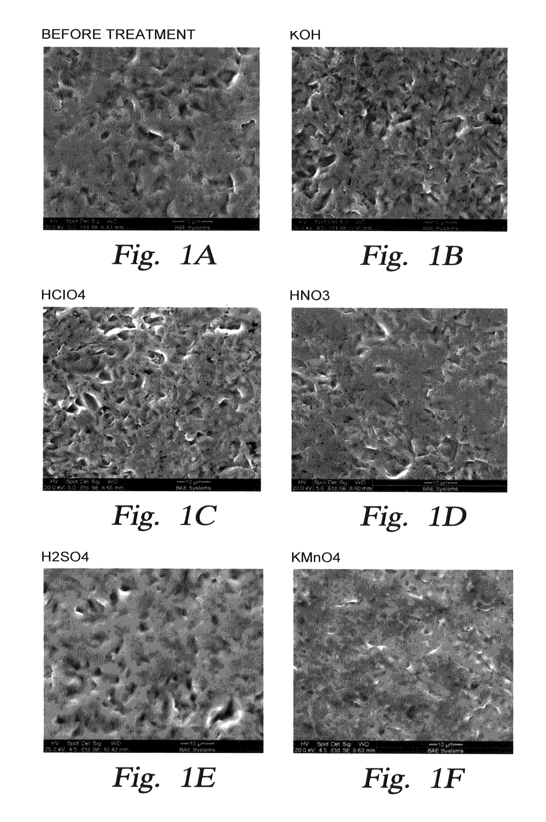
[0039]FIGS. 1A through 1F show comparison photomicrographs of the surface of CVD silicon carbide bulk test specimens which were exposed to a wet treatment by various oxidizing agents for 96 hours at 66° C., with the exception of the H2O2 and H2SO4 oxidizing agent, where the exposure time was 4 hours at 92° C. A smoother, more rounded topography generally indicates that there has been more reaction with the wet oxidizing solution, as confirmed by the measurement of changes in weight of the test specimens. The test specimens measured 10.031 mm in length, 2.062 mm width, and were 1 mm thickness. The weight of an individual test specimen was about 0.65 g, and the total surface area per specimen was 2.839776 cm.

[0040]FIG. 1A shows a photomicrograph of the silicon carbide surface after machining, where the surface was diamond grinded using a technique commonly known in the art. One and a half cm on the photomicrograph represents a distance of about 10 μm. The surface has a general roughne...

example two

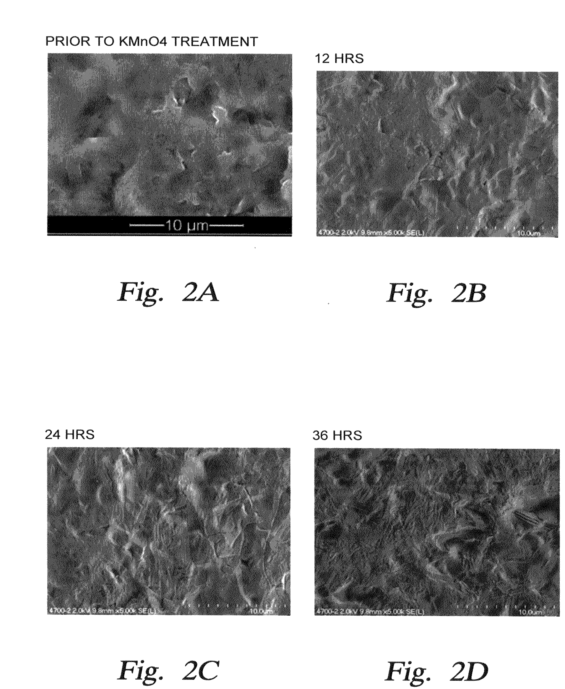
[0049]Test results related to Example One indicated that KMnO4 and the mixture of H2O2+H2SO4 were the most promising wet treatment oxidation agents based on data for weight changes and microstructural morphology; and, based on surface profile measurements which indicated flatness of the surface after the silicon oxide layer was stripped off using the hydrofluoric acid solution.

[0050]The surface profile measurements were made using surface profilometry measurement length scan (Pmrc %). The Pmrc is the length of bearing surface, i.e., the surface that is in direct contact with the profilometer tip, expressed as a percentage of the evaluation length at a nominal depth below the highest peak. The technique of Pmrc measurement is well known in the art. Pmrc data compliments the SEM examination as an indication of whether the surface has become more smooth. The higher the Pmrc value, the more smooth the length / area of that particular measurement. Typically, a minimum of 11 length / area sca...

example three

[0059]Evaluation of surface oxidation of the bulk CVD silicon carbide test specimen surfaces using the H2O2+H2SO4 mixture was also further investigated. In particular, the silicon carbide test specimen surfaces were treated with the H2O2+H2SO4 mixture 3 times, where the soaking time period in the mixture was 4 hours each time, and where the mixture was replaced with fresh H2O2+H2SO4 after each treatment. The temperature in the soaking bath was 90° C., and there was no ultrasonic vibration induced within the bath. The average change in weight for the six test specimens was a decrease of 0.00053% after the 12 hours of treatment.

[0060]A comparison of the 12 hour treatment using the H2O2+H2SO4 mixture solution with the 12 hour treatment using the KMnO4 solution indicated that the KMnO4 solution produced an oxide layer which was about 20% thicker. As a result, the KMnO4 solution looks more promising at this time, but if the processing conditions are optimized for the H2O2+H2SO4 mixture, ...


PUM

PropertyMeasurementUnit
Temperatureaaaaaaaaaa

Abstract

Method of removing damaged silicon carbide crystalline structure from the surface of a silicon carbide component. The method comprises at least two liquid chemical treatment processes, where one treatment converts silicon carbide to silicon oxide, and another treatment removes silicon oxide. The liquid chemical treatments are typically carried out at a temperature below about 100° C. The time period required to carry out the method is generally less than about 100 hours.

Description

BACKGROUND[0001]1. Field[0002]Embodiments of the present application relate to the use of chemical solution treatments to remove damaged crystalline structure from the surface of silicon carbide components in general, and in particular from the surface of silicon carbide components of the kind used as semiconductor processing apparatus.[0003]2. Description of Background Art[0004]This section describes background subject matter related to the present invention. There is no intention, either express or implied, that the background art discussed in this section legally constitutes prior art.[0005]Corrosion (including erosion) resistance is a critical property for apparatus components used in semiconductor processing chambers where corrosive environments are present, such as in plasma cleaning and etch processes, and in plasma-enhanced chemical vapor deposition processes. This is especially true where high-energy plasma is present and combined with chemical reactivity to act upon the su...

Claims


Application Information

Patent Timeline
IPC IPC(8): H01L21/302C01B31/36
CPCC04B41/009C04B41/5353C04B41/91C23C16/4404C04B35/565H01L21/302H01L21/3063
Inventor SUN, JENNIFER Y.CHOU, IRENE A.XU, LICOLLINS, KENNETH S.GRAVES, THOMAS
Owner FUJIFILM IMAGING COLORANTS
Why Eureka
Try Eureka