Heat Spreader in Multilayer Build Ups

a heat spreader and multi-layer technology, applied in the field of connection systems, can solve the problems of increasing energy consumption, hot spots on the pcb, limiting the applicability of electronic devices in a plurality of directions, etc., and achieve the effect of increasing the lifetime of components and improving thermal managemen

Inactive Publication Date: 2017-03-16
AT & S AUSTRIA TECH & SYSTTECHN AG
View PDF32 Cites 1 Cited by
  • Summary
  • Abstract
  • Description
  • Claims
  • Application Information

AI Technical Summary

Benefits of technology

The present invention provides a connection system for electronic components with enhanced thermal management. This allows for further miniaturization and increasing the lifetime of components. The system uses matrix-free materials that offer a high thermal conductivity compared to other materials, which enhances the lifetime of components. The heat distributing layer in the connection system effectively distributes heat and prevents hot spots on the components, especially in mobile devices. The heat distributing layer spreads along the entire connection system, providing a highly effective heat transfer. The system also allows for an improved thermal management and efficient electrical connection of electrically conductive layers.

Problems solved by technology

There is, however, a constant need for further miniaturization in the electronic industry in order to provide consumers and professionals with ever smaller yet more capable electronic devices and installations which require more electronic components to be packaged in a smaller space, leading to higher density of interconnection, multilayer build ups and active and passive component embedding, thus increasing the energy consumption and causing hot spots on a PCB.
This measurements are in fact very effective but do require considerable amount of space and add to the weight of the components, thus limiting its applicability in a plurality of electronic devices, such as mobile devices and in particular smart phones for instance.

Method used


Image

  • Heat Spreader in Multilayer Build Ups
  • Heat Spreader in Multilayer Build Ups
  • Heat Spreader in Multilayer Build Ups

Examples


Embodiment Construction

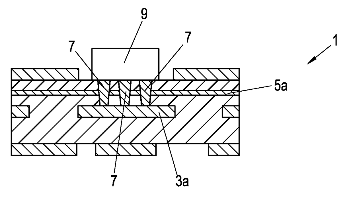
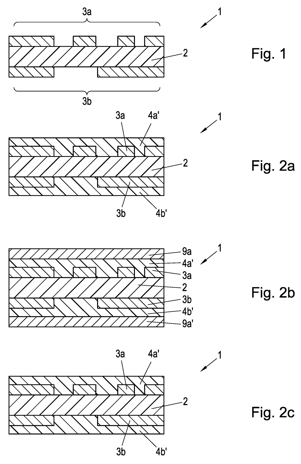
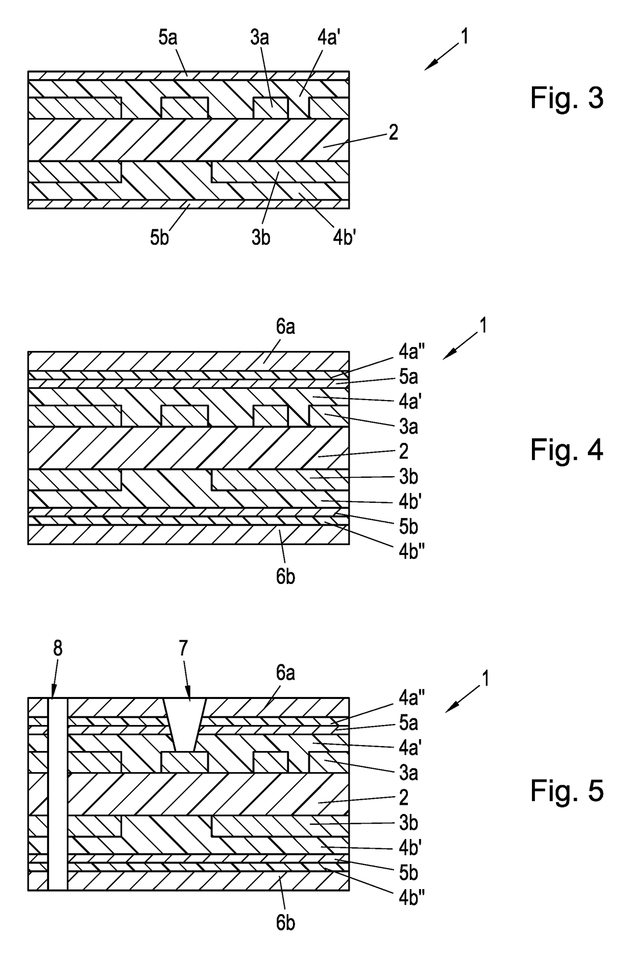
[0044]Embodiments of a connection system according to the invention as well as a method for producing the same will be described below in more detail with reference to the accompanying drawings. For same or similar components same reference numerals are used in order to avoid redundant explanations. The connection systems described in the exemplary embodiment is a printed circuit board. Of course, the connection system is not limited to PCBs but could also relates to other carrier planes (for example glass) in general not referred to as PCBs but being suited to provide an electrically insulating layer and at least one electrically conductive layer.

[0045]FIG. 1 shows a schematic cross-sectional view of a core of an exemplary PCB 1 prepared for a multilayer build up in a basic configuration. The PCB 1 according to FIG. 1 comprises an insulating layer 2, typically made of resin, and two structured conductive layers 3a and 3b, arranged on opposing sides of the insulating layer 2. The co...


PUM


Abstract

Connection system for electronic components, the connection system comprising at least one electrically insulating layer and at least one electrically conductive layer, wherein the connection system further comprises a heat distributing layer arranged within the at least one electrically insulating layer wherein the at least one heat distributing layer is made of thermally conductive, and electrically insulating, matrix-free material.

Description

FIELD OF THE INVENTION AND DESCRIPTION OF PRIOR ART[0001]The present invention relates to a connection system for electronic components, the connection system comprising at least one electrically insulating layer and at least one electrically conductive layer. Furthermore, the present invention relates to a method for producing a connection system.[0002]The invention relates to connection systems for electronic components in general, wherein electronic components such as transistors, integrated circuits (chips) and the like are arranged on or within a panel carrying and electrically connecting electronic components. Such panels are typically embodied as part of a printed circuit board. Alternatively, these carrying panels can be panels made of glass or any other insulating material suited to form a carrying panel. For the sake of simplicity, the description refers mostly to printed circuit boards. The person skilled in the art will, however, appreciate that whenever reference is mad...

Claims


Application Information

Patent Timeline
IPC IPC(8): H05K1/02H05K1/18H05K1/11
CPCH05K1/0207H05K1/0206H05K2201/0323H05K1/183H05K1/115H05K1/0203H05K1/0271H05K1/036H05K2201/0195H05K2201/068H05K3/4673H05K2201/0175
Inventor SCHULZ, GERNOTKREUTZWIESNER, ELISABETH
Owner AT & S AUSTRIA TECH & SYSTTECHN AG
Why Eureka
Try Eureka