
Surface-emitting laser and optical apparatus formed by using surface-emitting laser

a laser and surface-emitting technology, applied in semiconductor lasers, lighting and heating devices, instruments, etc., can solve the problems of multi-longitudinal mode oscillation or longitudinal mode hopping, and achieve the effect of stable beam spot, and suppressing longitudinal mode hopping

Inactive Publication Date: 2009-05-28
CANON KK
View PDF8 Cites 27 Cited by
  • Summary
  • Abstract
  • Description
  • Claims
  • Application Information

AI Technical Summary

Benefits of technology

[0020]However, the inventors of the present invention found that the use of a long cavity length is accompanied by the following disadvantage.
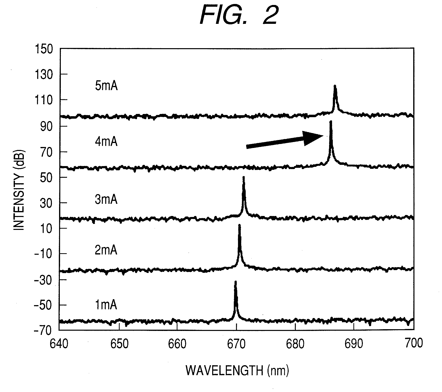
[0025]Referring to FIG. 2, the surface-emitting laser oscillates with a desired resonance wavelength in a region where the quantity of the injected electric current is small and not greater than 3 mA. However, it will be seen that the longitudinal mode hops to the next resonant mode (at 685 nm) as the injected electric current is raised above 4 mA in order to increase the light output.
[0027]In view of the above-identified problems, it is therefore an object of the present invention to provide a surface-emitting laser that can suppress longitudinal mode hopping and oscillate in a single longitudinal mode.
[0028]Another object of the present invention is to provide an optical apparatus that is formed by using a surface-emitting laser according to the present invention and can produce a stable beam spot.
[0029]Thus, a surface-emitting laser according to the present invention can oscillate in a single longitudinal mode, suppressing longitudinal mode hopping.

Problems solved by technology

Namely, there arises a problem of multi-longitudinal mode oscillation or that of longitudinal mode hopping, which is insignificant in conventional surface-emitting lasers.

Method used


Image

  • Surface-emitting laser and optical apparatus formed by using surface-emitting laser
  • Surface-emitting laser and optical apparatus formed by using surface-emitting laser
  • Surface-emitting laser and optical apparatus formed by using surface-emitting laser

Examples


first embodiment

[0066](Overall Configuration)

[0067]The configuration of the first embodiment, which is a surface-emitting laser that operates in a resonant mode of 680 nm, will be described below.

[0068]FIG. 3 is a schematic cross sectional view of the first embodiment, which is a red surface-emitting laser, illustrating the layer structure thereof.

[0069]Referring to FIG. 3, the red surface-emitting laser has an n-type GaAs substrate 322, a lower distributed Bragg reflector 302, a first cavity section 304, a second cavity section 306 and an upper distributed Bragg reflector 308.

[0070]More specifically, the lower distributed Bragg reflector 302 is formed by laying films of n-type AlAS and those of n-type Al0.5Ga0.5As to a predetermined thickness. Similarly, the upper distributed Bragg reflector 308 is formed by laying films of p-type Al0.9Ga0.1As and those of p-type Al0.5Ga0.5As to a predetermined thickness.

[0071]The first cavity section 304 is formed by using n-type Al0.9Ga0.1As. The second cavity s...

second embodiment

[0098]The second embodiment differs from the above-described first embodiment in that it is provided with a light absorption layer.

[0099]FIG. 6 is a schematic cross sectional view of the surface-emitting laser of the second embodiment, which is a red surface-emitting laser, illustrating the layer structure thereof.

[0100]The components of this embodiment same as those of the first embodiment illustrated in FIG. 3 are denoted respectively by the same reference symbols and will not be described here any further.

[0101]The difference between the surface-emitting laser of this embodiment and that (FIG. 3) of the first embodiment lies in the structure of the first cavity section 704.

[0102]Referring to FIG. 6, the first cavity section 704 of this embodiment is formed by two layers including a 2 μm-thick n-type Al0.35Ga0.65As layer 724 and a 2 μm-thick n-type Al0.9Ga0.1As layer 726. A layer that gives rise to absorption mainly on the basis of band-to-band transition in resonant modes (at 671...

third embodiment

[0121]The third embodiment is an optical apparatus formed by applying a surface-emitting laser according to the present invention, the configuration of which will be described below.

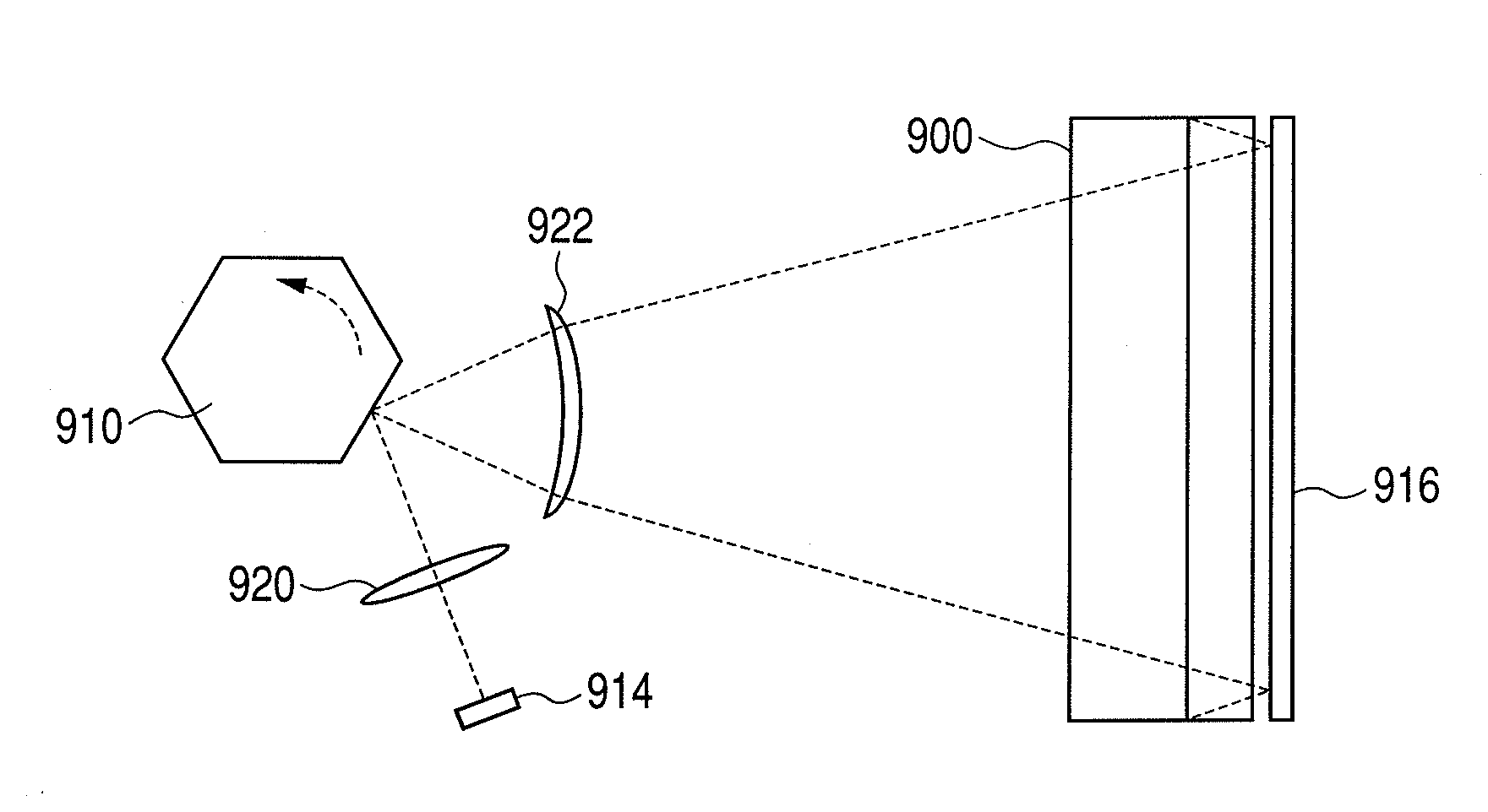
[0122]More specifically, an image-forming apparatus formed by using an array of red surface-emitting lasers according to the present invention will be described as an optical apparatus.

[0123]FIGS. 8A and 8B schematically illustrate an electrophotographic recording type image forming apparatus where a red surface-emitting laser array of this embodiment is installed.

[0124]FIG. 8A is a schematic plan view of the image forming apparatus and FIG. 8B is a schematic lateral view of the apparatus.

[0125]FIGS. 8A and 8B illustrate a photosensitive member 900, an electrostatic charger 902, a developer 904, a transfer charger 906, a fixer 908, a rotary polygon mirror 910 and a motor 912 as well as a red surface-emitting laser array 914, a reflector 916, a collimator lens 920 and a f-θ lens 922.

[0126]The image formin...


PUM


Abstract

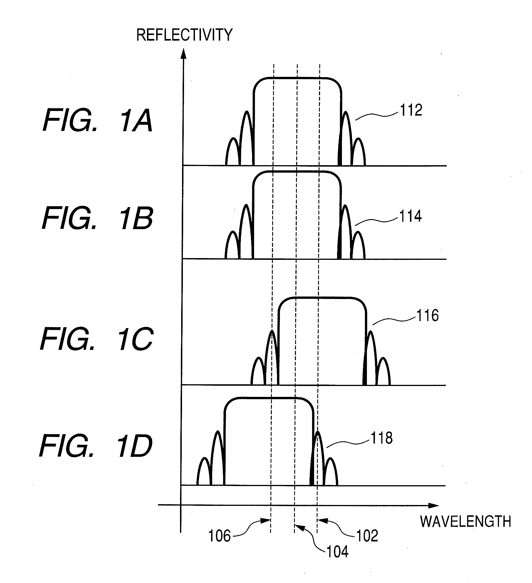
A surface-emitting laser has an active layer between a first distributed Bragg reflector and a second distributed Bragg reflector. The first distributed Bragg reflector is formed so as to have a resonant mode and a first longitudinal mode different from the resonant mode included in the reflectivity stop band and a second longitudinal mode different from the resonant mode and the first longitudinal mode excluded from the reflectivity stop band. Oscillation is suppressed in the first longitudinal mode and in the second longitudinal mode. As a result, the surface-emitting laser can oscillate in a single longitudinal mode, suppressing longitudinal mode hopping.

Description

BACKGROUND OF THE INVENTION[0001]1. Field of the Invention[0002]This invention relates to a surface-emitting laser and an optical apparatus formed by using a surface-emitting laser.[0003]2. Description of the Related Art[0004]A two-dimensional array of vertical cavity surface-emitting lasers (VCSELs) can be formed with ease. Then, light can be taken out from each of them in a direction perpendicular to the surface of the semiconductor substrate thereof.[0005]Thus, a plurality of beams of light emitted from such a two-dimensional array can be utilized for parallel processing for the purpose of densification and high speed operations. Therefore, surface-emitting lasers are expected to find various industrial applications.[0006]For example, a high density and high speed printing process can be realized by means of a plurality of beams for an electrophotographic printer when a surface-emitting laser array is employed as exposure light source for the electrophotographic printer.[0007]How...

Claims


Application Information

Patent Timeline
Patent Type & Authority Applications(United States)
IPC IPC(8): H01S5/187H01S5/183
CPCB82Y20/00H01S5/1039H01S2301/163H01S5/34326H01S5/18358
Inventor TAKEUCHI, TETSUYAUCHIDA, TAKESHI
Owner CANON KK
Learn More