Complementary semiconductor device and method of manufacturing the same
a semiconductor and semiconductor technology, applied in the field of complementary semiconductor devices, can solve problems such as the increase of manufacturing costs
- Summary
- Abstract
- Description
- Claims
- Application Information
AI Technical Summary
Benefits of technology
Problems solved by technology
Method used
Image


Examples
first embodiment
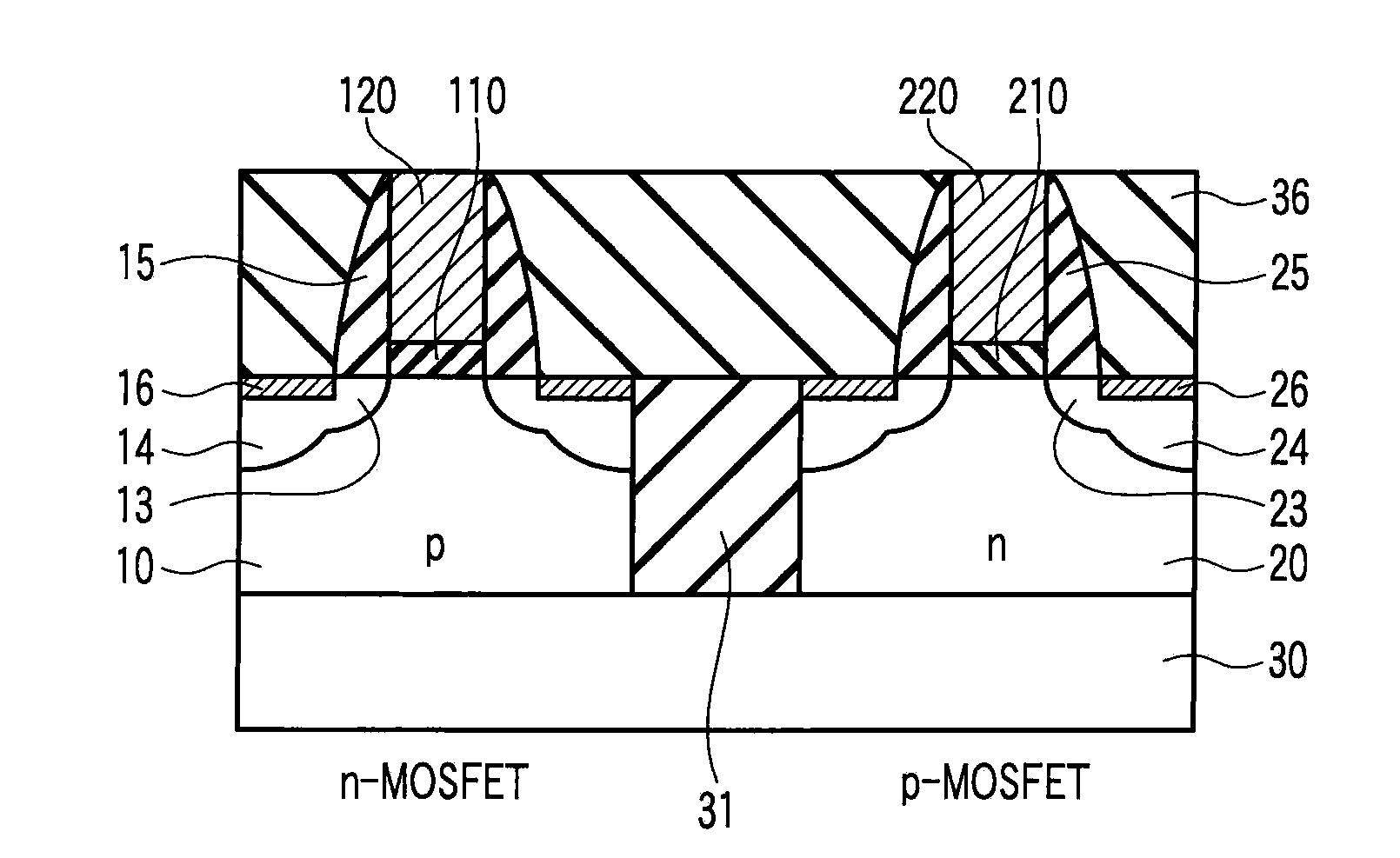
[0055]FIG. 7 is a cross-sectional view schematically showing the structure of a complementary semiconductor device (CMOS transistor) according to a first embodiment of the present invention. An Si substrate 30 is formed with p-type and n-type Si regions 10 and 20 via a device isolation insulating film 31. A substrate having a silicon-on-insulator (SOI) structure may be used as the foregoing substrate. An n-MOS transistor is formed on the p-type Si region (first semiconductor region) 10 while a p-MOS transistor is formed on the n-type Si region (second semiconductor region) 20.
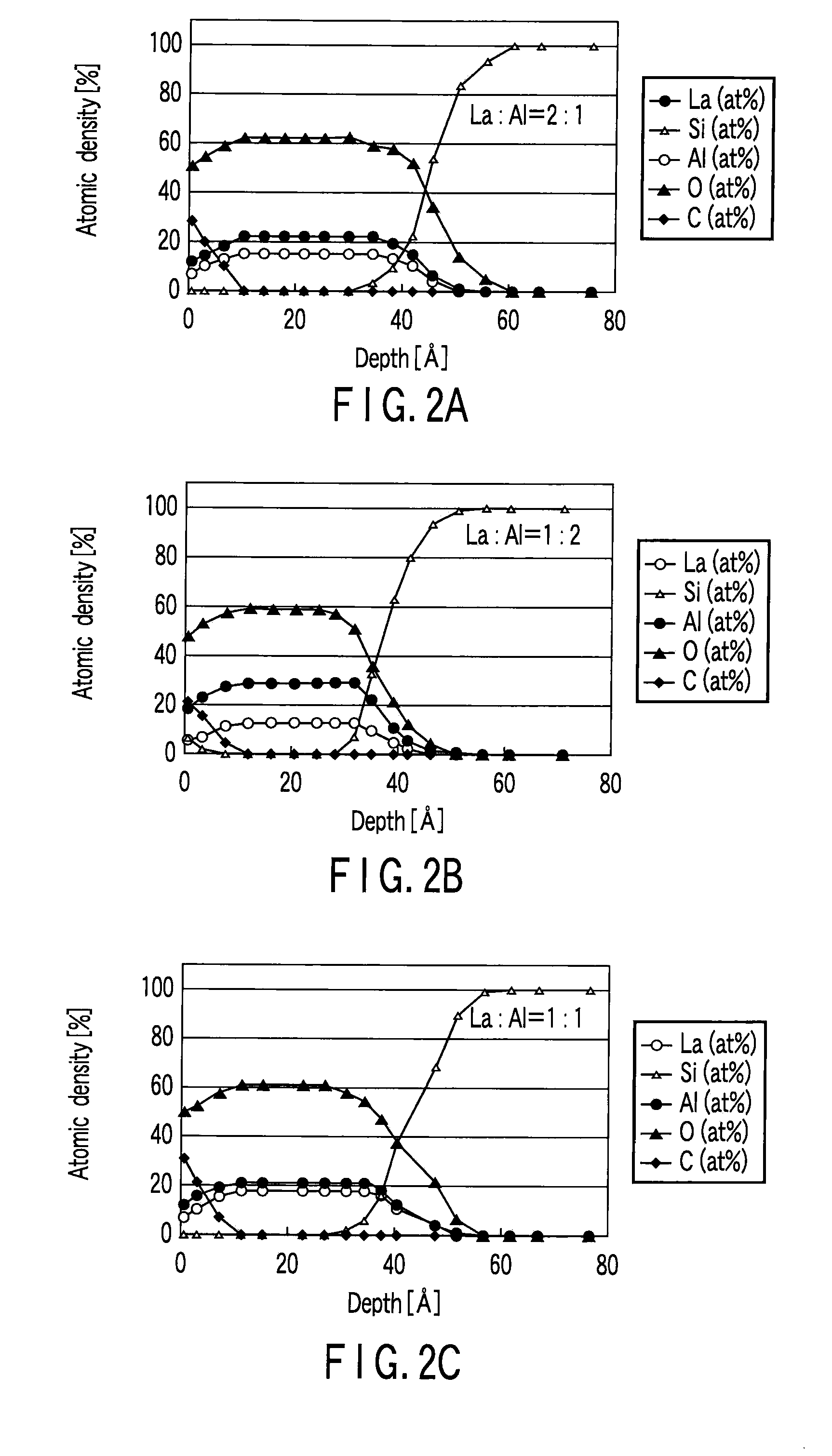
[0056]In the n-MOS transistor, an amorphous LaAlO3 film having a concentration ratio of Al / La=1 is deposited as a gate insulating film (first gate insulating film) 11 on the p-type Si region 10 without having a SiO2 interface layer. A gate electrode (first gate electrode) 12 including TaC is formed on the gate insulating film 11. The side portion of the gate insulating film 11 and the gate electrode 12 is forme...
second embodiment
[0082]FIGS. 9A to 9E are cross-sectional views showing a process of manufacturing a CMOS transistor according to a second embodiment of the present invention.
[0083]The second embodiment relates to a process of manufacturing a CMOS transistor forming a gate insulating film before a source / drain region is formed. The final structure of the CMOS transistor is the same as the first embodiment.
[0084]In the same manner as the first embodiment, a device isolation region 31 including a silicon oxide layer is formed on the boundary surface between p-type and n-type Si regions 10 and 20. Thereafter, as shown in FIG. 9A, a resist mask material 41 is formed on regions exclusive of a surface formed with a gate insulating film of the p-MOS transistor. Then, an amorphous LaAlO3 film 42 having Al / La concentration ratio=1.5 is formed as a gate insulating film 21 of the p-MOS transistor to have a thickness of about 3 nm using known process such as CVD and sputtering. Thereafter, the resist mask mater...
third embodiment
[0091]FIGS. 10A to 10C are cross-sectional views showing a process of manufacturing a CMOS transistor according to a third embodiment of the present invention.
[0092]The third embodiment relates to a method of manufacturing a CMOS transistor, which sets an Al / La concentration ratio of a gate insulating film of a p-MOS transistor higher than that of gate insulating film of an n-MOS transistor by Al ion implantation. The structure of the CMOS transistor is the same as the first embodiment.
[0093]As shown in FIG. 10A, a device isolation layer 31 including a silicon oxide is formed at the boundary surface between p-type and n-type Si regions 10 and 20, like the foregoing first embodiment. Then, an amorphous LaAlO3 film 51 having an Al / La concentration ratio=1 is deposited as a gate insulating film on the device isolation layer 31 formed between p-type and n-type Si regions 10 and 20 to have a thickness of about 3 nm. A TaC film 52 is further deposited as a gate electrode on the film 51.
[0...
PUM
 Abstract
Description
Claims
Application Information
 - R&D
- Intellectual Property
- Life Sciences
- Materials
- Tech Scout
- Unparalleled Data Quality
- Higher Quality Content
- 60% Fewer Hallucinations
Browse by: Latest US Patents, China's latest patents, Technical Efficacy Thesaurus, Application Domain, Technology Topic, Popular Technical Reports.
© 2025 PatSnap. All rights reserved.Legal|Privacy policy|Modern Slavery Act Transparency Statement|Sitemap|About US| Contact US: help@patsnap.com