
Laminated conductive film, electro-optical display device and production method of same

a technology of electro-optical display and conductive film, which is applied in the direction of superimposed coating process, insulation conductor/cable, instruments, etc., can solve the problems of increasing the number of production steps, reducing production efficiency, and difficulty in recognizing the display, and achieves superior electro-optical properties

Inactive Publication Date: 2009-04-30
MITSUBISHI ELECTRIC CORP
View PDF5 Cites 24 Cited by
  • Summary
  • Abstract
  • Description
  • Claims
  • Application Information

AI Technical Summary

Benefits of technology

[0026]According to the present invention, a laminated conductive film comprising a transparent conductive film and Al-based film can be provided that is capable of realizing a high-quality film with superior electro-optical properties, without providing a buffer layer or protective layer. In addition, a method of producing the above-mentioned laminated conductive film can also be provided. Moreover, an electro-optical display device that uses this laminated conductive film, and a production method thereof, can also be provided.

Problems solved by technology

However, this type of transmissive liquid crystal display panel made it difficult to recognize the display as a result of the display light of the display panel appearing darker than the surrounding light when used outdoors during the day when surrounding light is extremely bright.
Consequently, it has the shortcomings of causing an increase in the number of production steps and a decrease in production efficiency.
However, in the production method as described above as well, not only was it difficult to form a structure in which Al and ITO are laminated directly, but as is also described in Japanese Unexamined Patent Application Publication NO.
As a result, oxidative corrosion of the Al and reductive corrosion of the ITO occur.
Consequently, display defects occur caused by film separation and deterioration of the transmittance of the transmissive electrode in the form of the ITO film.
Consequently, electrical continuity between the Al and ITO is impaired.
Electrical signals between the transmissive electrode and reflective electrode are interrupted resulting in a defective display.
However, when the inventors of the present invention deposited an AlNi-based alloy directly on an ITO (90% by weight indium oxide+10% by weight tin oxide) film, a large number of film defects in the shape of round spots were determined to occur when viewed with a light microscope.
At the locations of these round spot-shaped defects, the film was damaged by metal In and metal Sn reduced on the ITO film below resulting in partial separation of the film.
Namely, although electrical continuity at the interface between the AlNi and ITO is improved due to the presence of metal In and metal Sn reduced near the interface, spot-shaped defects are thought to have occurred due to this phenomenon.
In the case of using a laminated conductive film comprising the deposition of an AlNi-based alloy film on an ITO film as a pixel electrode of a display, these spot-shaped defects become a fatal problem since they lead directly to a defective display.
However, ZnO-based films have inferior optical transmittance and specific resistance as compared with ITO films.
Consequently, display properties are inferior in the case of using a ZnO-based film for a pixel electrode.
Moreover, since ZnO-based films are violently corroded and etched by typically known etching solutions of Al-based metals in the form of phosphoric acid, nitric acid and acetic acid-based chemical solutions, it is extremely difficult to simultaneously carry out wet etching processing on Al-based films and ZnO-based films.
Thus, it was substantially impossible to use ZnO-based films as transparent conductive films.
As has been described above, since it is necessary to form a transmissive electrode and reflective electrode for the pixel electrodes in the case of conventionally known semi-transmissive liquid crystal display devices, there were problems in the form of an increase in the number of production steps and decreased production efficiency.
In addition, in the case of attempting to form the transmissive electrode and reflective electrode collectively, it is difficult to produce an ITO or other oxide transparent conductive film serving as a transmissive electrode and high reflectance Al-based alloy film serving as a reflective electrode in the form of a directly laminated film using conventionally known production methods, and since it was necessary to form an additional metal buffer layer between the Al and ITO, this resulted in the problems of an increase in the number of deposition steps and decreased production efficiency.

Method used


Image

  • Laminated conductive film, electro-optical display device and production method of same
  • Laminated conductive film, electro-optical display device and production method of same
  • Laminated conductive film, electro-optical display device and production method of same

Examples


first embodiment

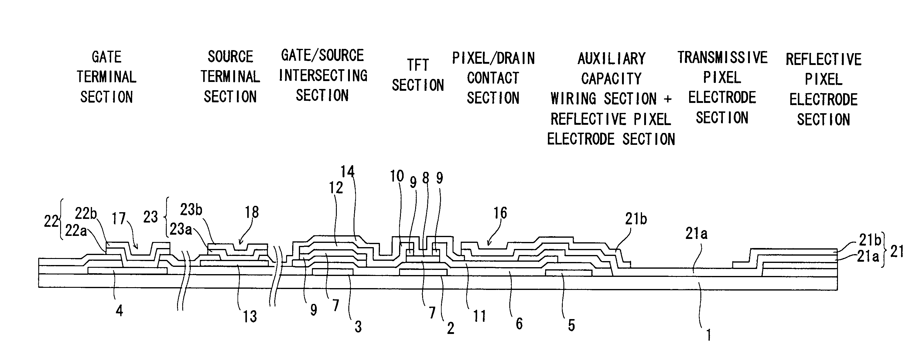
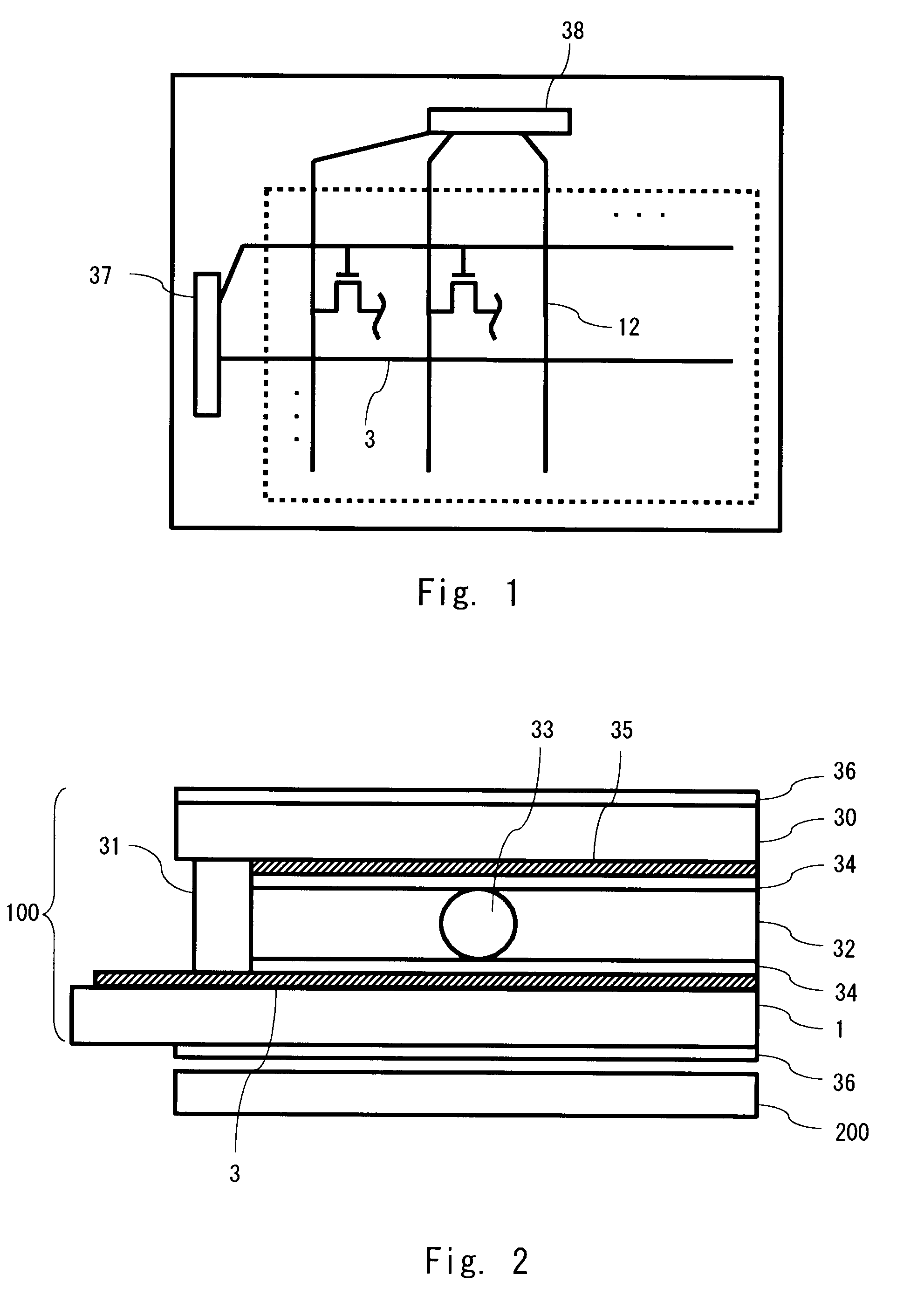
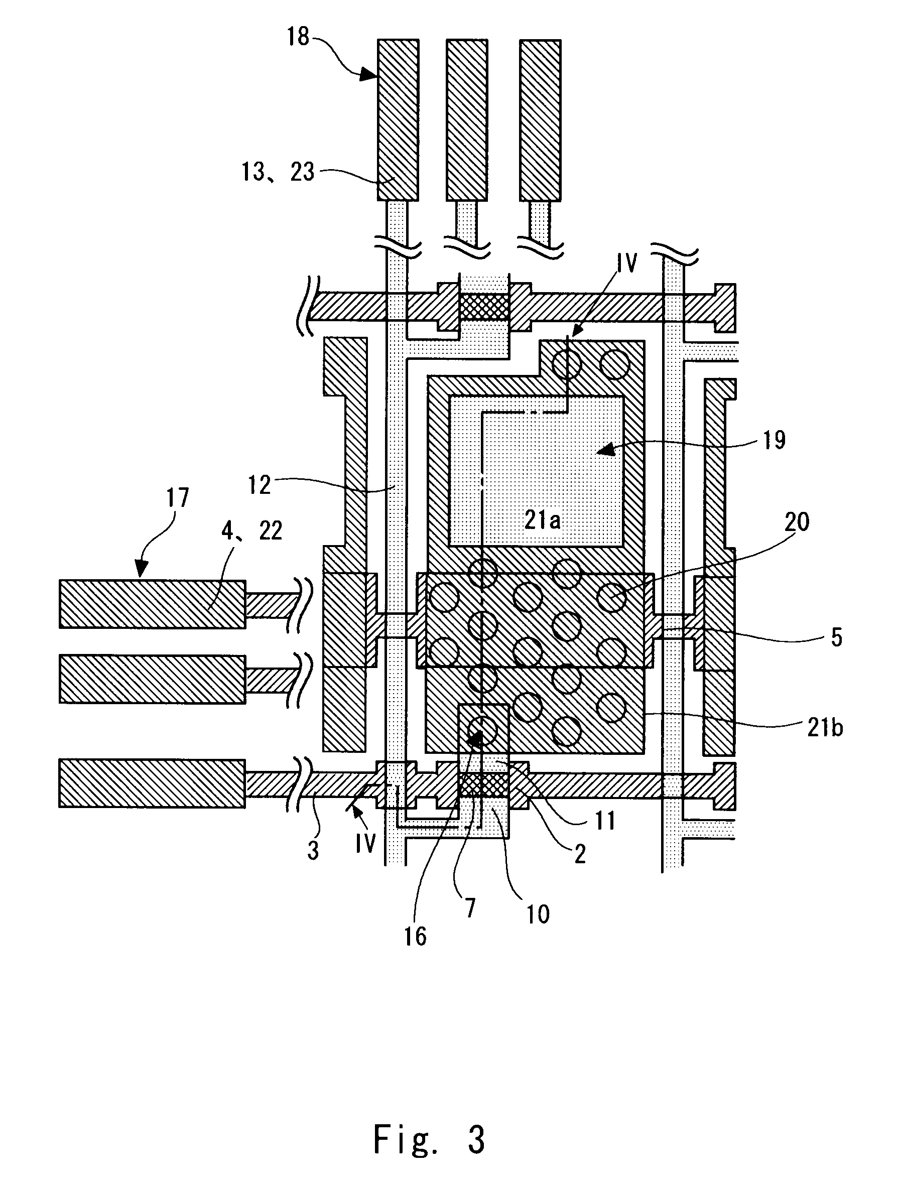
[0036]The following provides an explanation of the configuration of a semi-transmissive liquid crystal display device, and production method thereof, as an electro-optical display device according to a first embodiment of the present invention with reference to the drawings. First, with reference to FIGS. 1 and 2, an explanation is provided of the configuration of a semi-transmissive liquid crystal display device according to the present embodiment. FIG. 1 is an overhead view showing the configuration of a semi-transmissive liquid crystal display device according to the present embodiment. In addition, FIG. 2 is a cross-sectional view showing the configuration of a semi-transmissive liquid crystal display device according to the present embodiment.

[0037]As shown in FIGS. 1 and 2, a semi-transmissive liquid crystal display according to the present embodiment is provided with a liquid crystal display panel 100 and a backlight 200. The liquid crystal display panel 100 displays images b...

second embodiment

[0078]An electro-optical display device according to a second embodiment of the present invention has a TFT active matrix substrate of the same configuration as that used in the semi-transmissive liquid crystal display device of the first embodiment shown in FIGS. 3 and 4. In addition, although the basic process flows of the production method thereof is also the same as that of the first embodiment as shown in FIGS. 5A to 5H, the method of forming the pixel electrode 21 shown in FIG. 5E differs from that of the first embodiment. The following provides a detailed explanation of that difference in the production method.

[0079]In the pixel electrode formation step shown in FIG. 5E, the transparent conductive film 21a is first deposited on the second interlayer insulating film 15. Subsequently, plasma comprised mainly of air is irradiated onto the surface of this transparent conductive film 21a. A third metal conductive film is then deposited on the transparent conductive film 21a irradi...

third embodiment

[0083]The following provides an explanation of the configuration of a TFT active matrix substrate used in an electro-optical display device according to a third embodiment of the present invention with reference to FIG. 6. FIG. 6 is a cross-sectional view showing the configuration of the TFT active matrix substrate according to the present embodiment. In the present embodiment, the second interlayer insulating film 15 of the first and second embodiments is omitted, and surface irregularities for scattering reflected light are not formed on the reflective pixel electrode. In addition, the production method thereof is able to use the production flow of the first and second embodiments with the exception of omitting the formation of the second interlayer insulating film 15. Thus, the production process can be simplified thereby making it possible to further improve production efficiency.

[0084]The optical path lengths of the reflective pixel electrode section and the transmissive pixel ...


PUM

PropertyMeasurementUnit
transmittanceaaaaaaaaaa
thicknessaaaaaaaaaa

Abstract

The present invention provides a laminated conductive film, comprising a transparent conductive film and Al-based film, that is capable of realizing a high-quality film with superior electro-optical properties, without providing a buffer layer or protective layer. A laminated conductive film according to one aspect of the present invention is provided with a transparent conductive film having optical transmissivity, and a metal conductive film laminated directly on the transparent conductive film and electrically connected to the transparent conductive film. The metal conductive film is made of Al or has Al as a main component thereof and contains at least one of nitrogen atom and oxygen atom at least in the vicinity of the interface with the transparent conductive film.

Description

BACKGROUND OF THE INVENTION[0001]1. Field of the Invention[0002]The present invention relates to a laminated conductive film having a transparent conductive film and to a production method thereof. In addition, the present invention relates to an electro-optical display device having a thin film transistor (TFT) and a pixel electrode, and to a production method thereof.[0003]2. Description of Related Art[0004]Electro-optical display devices, as exemplified by liquid crystal display devices and electroluminescence (EL) display devices, have the characteristics of a thin shape and low power consumption. Electro-optical display devices are widely used in applications such as the displays of cellular telephones, electronic assistants and other portable information devices, monitors of personal computer, image monitors of digital cameras and video cameras and, more recently, space-saving, large-screen TVs by taking advantage of these characteristics.[0005]Among these electro-optical disp...

Claims


Application Information

Patent Timeline
Patent Type & Authority Applications(United States)
IPC IPC(8): H01L21/77H01L27/088C23C16/513B32B15/04B32B9/00C23C14/34H01B13/06
CPCC23C26/00C23C28/00G02F2001/136295H01L27/124C23C28/04C23C28/321C23C28/345H01L27/12G02F1/136295Y10T428/31678
Inventor INOUE, KAZUNORIHAYASHI, MASAMIISHIGA, NOBUAKI
Owner MITSUBISHI ELECTRIC CORP
Learn More