Variable Inductance Applying Device Using Variable Capacitor and Variable Frequency Generating Device Thereof

a variable capacitor and inductance application technology, applied in the direction of continuous tuning, instruments, sport apparatus, etc., can solve the problems of energy loss, narrow variable range, and difficulty in adjusting the frequency through changing c, and achieve the effect of low energy loss

Inactive Publication Date: 2009-04-16
SAMSUNG ELECTRONICS CO LTD
View PDF5 Cites 3 Cited by
  • Summary
  • Abstract
  • Description
  • Claims
  • Application Information

AI Technical Summary

Benefits of technology

[0014]It is, therefore, an aspect of the present invention to provide a variable inductance applying device with a high value of quality factor Q, capable of applying inductance to a circuit in need of variable inductance with a low energy loss, and a variable frequency generating and processing device thereof.

Problems solved by technology

In such case, however, the variable range is very narrow.
Therefore, changing the frequency through changing C gives rise to problems especially in a multi-band communication system requiring a broad variable frequency range.
However, since a switching element such as the MOS transistor M includes a resistance component, it causes energy loss.
This results in an increase in the size of the resonance circuit.
However, the variable inductance applying device as shown in FIG. 2 does not address the energy loss problem caused by the resistance component in the switching element 30.

Method used


Image

  • Variable Inductance Applying Device Using Variable Capacitor and Variable Frequency Generating Device Thereof
  • Variable Inductance Applying Device Using Variable Capacitor and Variable Frequency Generating Device Thereof
  • Variable Inductance Applying Device Using Variable Capacitor and Variable Frequency Generating Device Thereof

Examples


Embodiment Construction

[0030]An exemplary embodiment of the present invention will be described herein below with reference to the accompanying drawings.

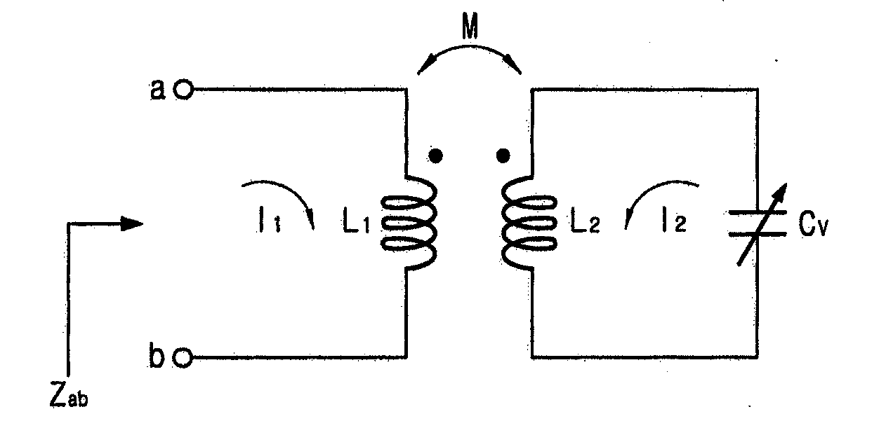
[0031]FIG. 3 is a circuit diagram of a variable inductance applying device, in accordance with one exemplary embodiment of the present invention. The variable inductance applying device applies inductance to a resonance circuit through an inductance applying terminal a-b. Referring to FIG. 3, the variable inductance applying device includes a main inductor L1, a sub inductor L2, and a variable capacitor Cv.

[0032]Both terminals of the main inductor L1 are connected to the inductance applying terminal a-b, whereas both terminals of the sub inductor L2 are connected to the variable capacitor Cv (to be described). Further, the main inductor L1 and the sub inductor L2 are inductively coupled to each other, and the mutual inductance between the two is labeled ‘M’.

[0033]There is no limitation on the arrangement or configuration of the main inductor L1 and the su...


PUM


Abstract

Disclosed is a variable inductance applying device using a variable capacitor, and a variable frequency generating device thereof. The variable inductance applying device includes: a first inductor whose both terminals are connected to an inductance applying terminal applying inductance to an external circuit; a second inductor inductively coupled to the first inductor; and a variable capacitor connected to both terminals of the second inductor, which varies inductance from the inductance applying terminal by changing capacitance. Therefore, the inductance to be applied to the external circuit can be varied by changing the capacitance of the variable capacitor. Since the variable capacitor rarely contains a resistance component, energy loss due to the resistance component hardly occurs. As a result, the variable inductance applying device has a high value of Q.

Description

CROSS-REFERENCE TO RELATED APPLICATIONS[0001]This application is a continuation of U.S. application Ser. No. 10 / 375,053 filed Feb. 24, 2006, the disclosure of which is incorporated herein by reference in its entirety. This application claims priority from Korean Patent Application No. 2005-16802, filed Feb. 28, 2005.BACKGROUND OF THE INVENTION[0002]1. Field of the Invention[0003]The present invention relates in general to a variable inductance applying device and a variable frequency generating device using the same. More specifically, the present invention relates to a variable inductance applying device applying inductance to a circuit in need of variable inductance, and a variable frequency generating thereof.[0004]2. Description of the Related Art[0005]For communication equipment to work, diverse ranges of frequencies are required. To this end, communication equipment must have a frequency generating and processing (amplification for example) device, which is realized by using a...

Claims


Application Information

Patent Timeline
Patent Type & Authority Applications(United States)
IPC IPC(8): H03J3/22
CPCH03J3/20H03B5/08A63C17/08A63C5/00
Inventor EO, YUN-SEONGLEE, KWANG-DULEE, HEUNG-BAE
Owner SAMSUNG ELECTRONICS CO LTD
Why Eureka
Try Eureka