Eureka AIR delivers breakthrough ideas for toughest innovation challenges, trusted by R&D personnel around the world.

System for Supporting Partial Cache Line Write Operations to a Memory Module to Reduce Write Data Traffic on a Memory Channel

a memory module and write operation technology, applied in the field of data processing system and method, can solve the problems of reducing operating costs, exacerbate the design challenges of memory system, increasing storage, etc., and achieve the effect of reducing the amount of bandwidth used, consuming bandwidth, and increasing the available bandwidth of a memory channel

Inactive Publication Date: 2009-03-05
IBM CORP
View PDF94 Cites 49 Cited by
  • Summary
  • Abstract
  • Description
  • Claims
  • Application Information

AI Technical Summary

Benefits of technology

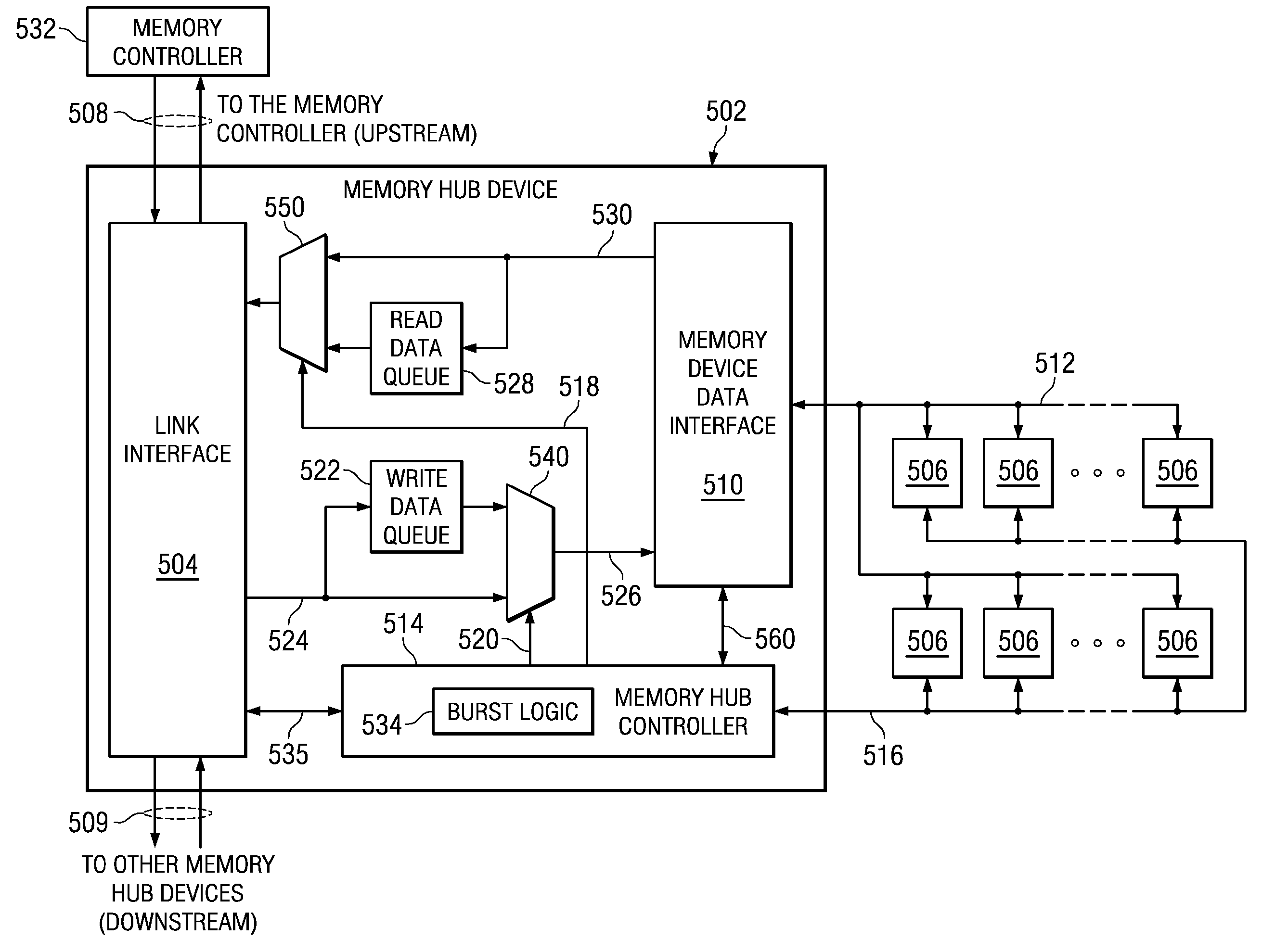
[0009]In order to increase the available bandwidth of a memory channel, the illustrative embodiments reduce the amount of bandwidth used during reading and writing of data from and to the memory system. Typically, when accessing data from a memory system using a cache mechanism, data transfers are performed in terms of entire cache lines even if the amount of data required by the read or write operation is only a sub-portion of the cache line. Thus, some data is transferred across the memory channel which is simply discarded. As a result, bandwidth is consumed by data traffic which contains data that is not used and hence, bandwidth is wasted in transferring this data.
[0010]The illustrative embodiments provide mechanisms for increasing the usable bandwidth of a memory system. One illustrative embodiment provides for supporting partial cache line read operations to a memory module to reduce read data traffic on a memory channel. Another illustrative embodiment provides for supporting partial cache line write operations to a memory module to reduce write data traffic on the memory channel. A further illustrative embodiment provides for increasing the available bandwidth on the memory channel by managing memory device error correction within a memory hub device. Yet another illustrative embodiment provides for a variable width memory device data interface to memory devices that allows additional error correction capability at the memory device level that is transparent to the memory channel.
[0013]In the illustrative embodiments, the memory hub controller may control the amount of write data that is transmitted by generating a data mask control signal based on the burst length field and transmits the data mask control signal to the memory device data interface at substantially a same time as data is input to the memory device data interface. In the illustrative embodiments, the data mask control signal may cause the memory device data interface to transmit, as valid write data, only a portion of the data input to the memory device data interface corresponding to the amount of write data determined by the burst logic.

Problems solved by technology

High-availability systems, i.e. systems that must be available to users without failure for large periods of time, present further challenges related to overall system reliability due to customer expectations that new computer systems will markedly surpass existing systems with regard to mean-time-before-failure (MTBF), in addition to offering additional functions, increased performance, increased storage, lower operating costs, etc.
Other frequent customer requirements further exacerbate the memory system design challenges, and include such items as ease of upgrade and reduced system environmental impact, such as space, power, and cooling.
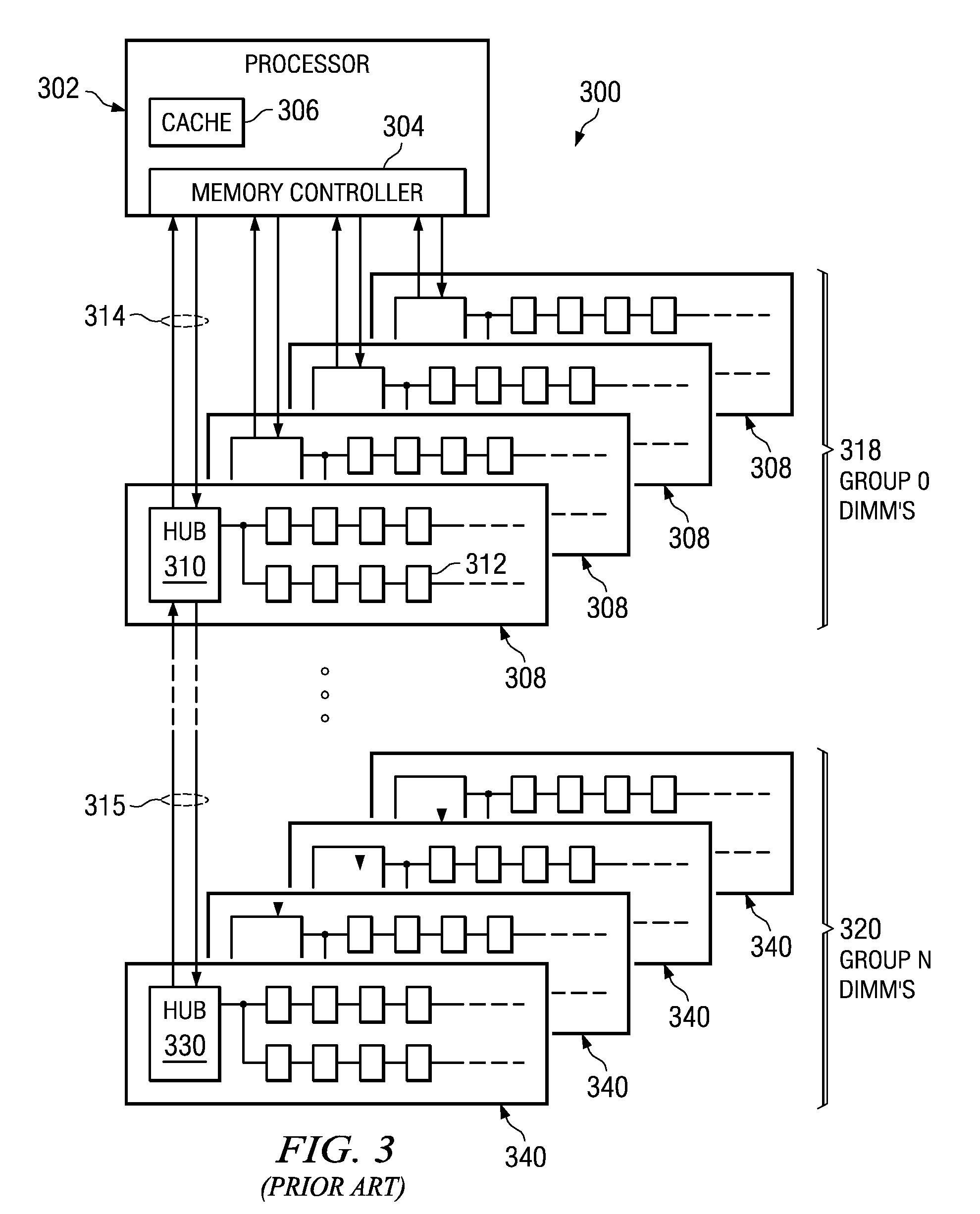
Thus, the memory channel presents a limiting factor, or bottleneck, for the flow of data to / from the memory modules of a memory system.
As a result, bandwidth is consumed by data traffic which contains data that is not used and hence, bandwidth is wasted in transferring this data.

Method used


Image

  • System for Supporting Partial Cache Line Write Operations to a Memory Module to Reduce Write Data Traffic on a Memory Channel
  • System for Supporting Partial Cache Line Write Operations to a Memory Module to Reduce Write Data Traffic on a Memory Channel
  • System for Supporting Partial Cache Line Write Operations to a Memory Module to Reduce Write Data Traffic on a Memory Channel

Examples


Embodiment Construction

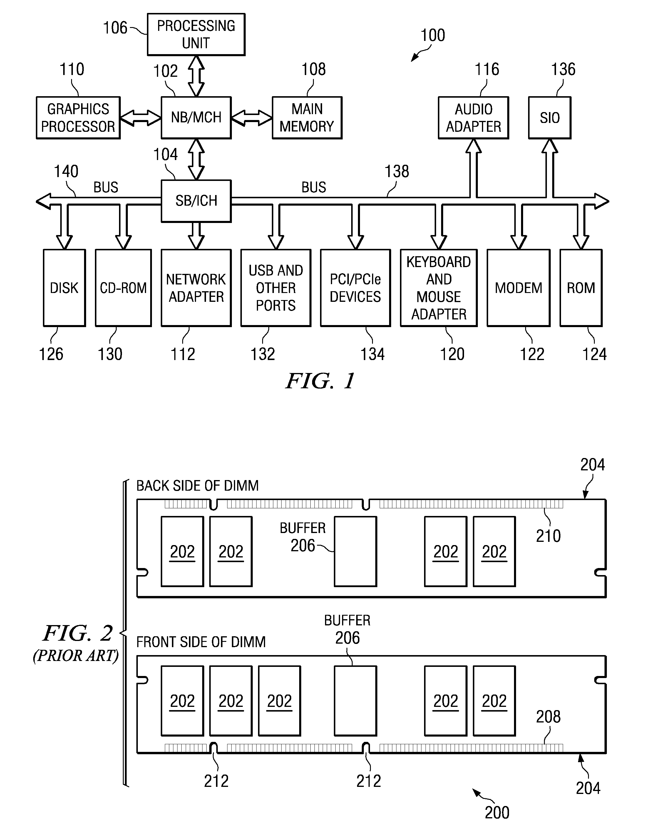
[0026]The illustrative embodiments provide mechanisms for enhancing the memory bandwidth available through a buffered memory module. As such, the mechanisms of the illustrative embodiments may be used with any of a number of different types of data processing devices and environments. For example, the memory system of the illustrative embodiments may be utilized with data processing devices such as servers, client data processing systems, stand-alone data processing systems, or any other type of data processing device. Moreover, the memory systems of the illustrative embodiments may be used in other electronic devices in which memories are utilized including printers, facsimile machines, storage devices, flash drives, or any other electronic device in which a memory is utilized. In order to provide a context for the description of the mechanisms of the illustrative embodiments, and one example of a device in which the illustrative embodiments may be implemented, FIG. 1 is provided h...


PUM


Abstract

A memory system is provided that supports partial cache line write operations to a memory module to reduce write data traffic on a memory channel. The memory system comprises a memory hub device integrated in the memory module and a set of memory devices coupled to the memory hub device. The memory hub device comprises burst logic integrated in the memory hub device. The burst logic determines an amount of write data to be transmitted to the set of memory devices and generates a burst length field corresponding to the amount of write data. The memory hub also comprises a memory hub controller integrated in the memory hub device. The memory hub controller controls the amount of write data that is transmitted using the burst length field. The memory hub device transmits the amount of write data that is equal to or less than a conventional data burst amount.

Description

GOVERNMENT RIGHTS[0001]This invention was made with Government support under DARPA, HR0011-07-9-0002. THE GOVERNMENT HAS CERTAIN RIGHTS IN THIS INVENTION.BACKGROUND[0002]1. Technical Field[0003]The present application relates generally to an improved data processing system and method. More specifically, the present application is directed to a system for supporting partial cache line write operations to a memory module to reduce write data traffic on a memory channel.[0004]2. Description of Related Art[0005]Contemporary high performance computing main memory systems are generally composed of one or more dynamic random access memory (DRAM) devices, which are connected to one or more processors via one or more memory control elements. Overall computer system performance is affected by each of the key elements of the computer structure, including the performance / structure of the processor(s), any memory cache(s), the input / output (I / O) subsystem(s), the efficiency of the memory control...

Claims


Application Information

Patent Timeline
IPC IPC(8): G06F12/08G06F13/14
CPCG06F13/161
Inventor GOWER, KEVIN C.MAULE, WARREN E.
Owner IBM CORP
Why Eureka
Eureka Blog
Learn More