CMOS Logic Compatible Non-Volatile Memory Cell Structure, Operation, And Array Configuration

a non-volatile memory, non-volatile technology, applied in static storage, digital storage, instruments, etc., can solve the problems of increased processing time, increased manufacturing cost, and increased possibility of defects, and achieve the effect of lowering the erase voltag

Active Publication Date: 2009-02-26
INFINEON TECH LLC
View PDF5 Cites 12 Cited by
  • Summary
  • Abstract
  • Description
  • Claims
  • Application Information

AI Technical Summary

Benefits of technology

[0021]To further lower the erase voltage, according to various aspects of the pre

Problems solved by technology

However, many NVM processes require multiple layers of poly-silicon, while many conventional CMOS processes require only a single layer of poly-silicon.
These additional processing steps result in increased processing time, higher cost of manufacturing, increased possibility of defects, and in turn result in lower yields.
But valuable areas on the die are consumed by these repair circuits, further increasing the cost of manufacturing.
In addition, the conventional EEPROM cell structure creates manufacturing difficulties.
As a result, the manufacturing cost of the conventional EEPROM is higher, the cell size is bigger, and the array density is limited to low density devices.
Additionally, the complex topology of the conventional EE

Method used


Image

  • CMOS Logic Compatible Non-Volatile Memory Cell Structure, Operation, And Array Configuration
  • CMOS Logic Compatible Non-Volatile Memory Cell Structure, Operation, And Array Configuration
  • CMOS Logic Compatible Non-Volatile Memory Cell Structure, Operation, And Array Configuration

Examples


Embodiment Construction

[0029]Whereas many alterations and modifications of the present invention will become apparent to persons of ordinary skills in the art after having read the foregoing description, it is to be understood that any particular embodiment shown and described by way of illustration is in no way intended to be considered limiting. Therefore, references to details of various embodiments are not intended to limit the scope of the claims which in themselves recite only those features regarded as the invention.

[0030]In this description and claims, the terms “coupled” and “connected”, along with their derivatives, may be used. It should be understood that these terms are not intended as synonyms for each other. Rather, in particular embodiments, “connected” may be used to indicate that two or more elements are in direct physical or electrical contact with each other. “Coupled” may mean that two or more elements are either in direct physical or electrical contact or that two or more elements ar...


PUM


Abstract

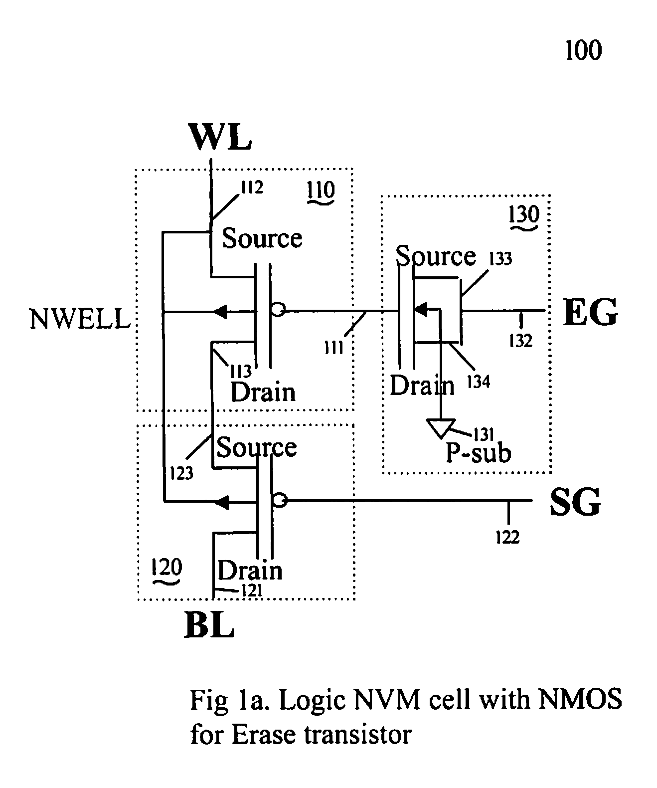
The present invention is to provide a logic based single-poly non-volatile memory cell which is compatible with the CMOS process, uses lower voltages for operating, and is more reliable in program, read, or erase operation. A non-volatile memory cell in accordance with the present invention comprises a program transistor with a program transistor source as a first program terminal; a select transistor with a select transistor gate as a select terminal and a select transistor drain as a second program terminal; and an erase transistor with an erase transistor source and an erase transistor drain connected as an erase terminal, wherein the erase transistor shares a floating gate with the program transistor and the drain program transistor is connected to the select transistor source. By employing the present invention, significant cost advantages in feature-rich semiconductor products, such as System-on-Chip (SoC) design, compared to conventional dual-poly floating gate embedded Flash memory are provided.

Description

TECHNICAL FIELD [0001]The present invention relates to non-volatile memory (NVM), and more particularly, to a CMOS Logic based non-volatile memory (NVM) which is made directly with CMOS logic process without any additional mask or process step.BACKGROUND ARTS [0002]NVM is now widely used for a variety of applications, since it may store information without continuously applied electric power, and by applying appropriate voltages, the NVM may be programmed or re-programmed (erased). Such a memory may provide a basic operating system or microcode for a logic device, such as a processor. A kind of NVM, embedded NVM in a CMOS device, allows a single chip produced by a manufacturer to be configured for various applications, and / or allows a single device to be configured by a user for different applications. Programming of the embedded NVM is typically done by downloading code from an external source, such as a computer.[0003]However, many NVM processes require multiple layers of poly-sil...

Claims


Application Information

Patent Timeline
IPC IPC(8): G11C11/40
CPCG11C2216/10G11C16/0433
Inventor LI, DANIEL D.ZHOU, STEVE X.
Owner INFINEON TECH LLC
Why Eureka
Try Eureka