Semiconductor device
a technology of semiconductor devices and shielding devices, which is applied in the direction of semiconductor devices, semiconductor/solid-state device details, electrical apparatus, etc., can solve the problems of increasing the current consumption at standby during the entire operation of the integrated circuit, the current of the off transistor is much more serious, and the protection function cannot be sufficiently implemented, so as to prevent the generation of esd, and maintain the leakage current small
- Summary
- Abstract
- Description
- Claims
- Application Information
AI Technical Summary
Benefits of technology
Problems solved by technology
Method used
Image


Examples
first embodiment
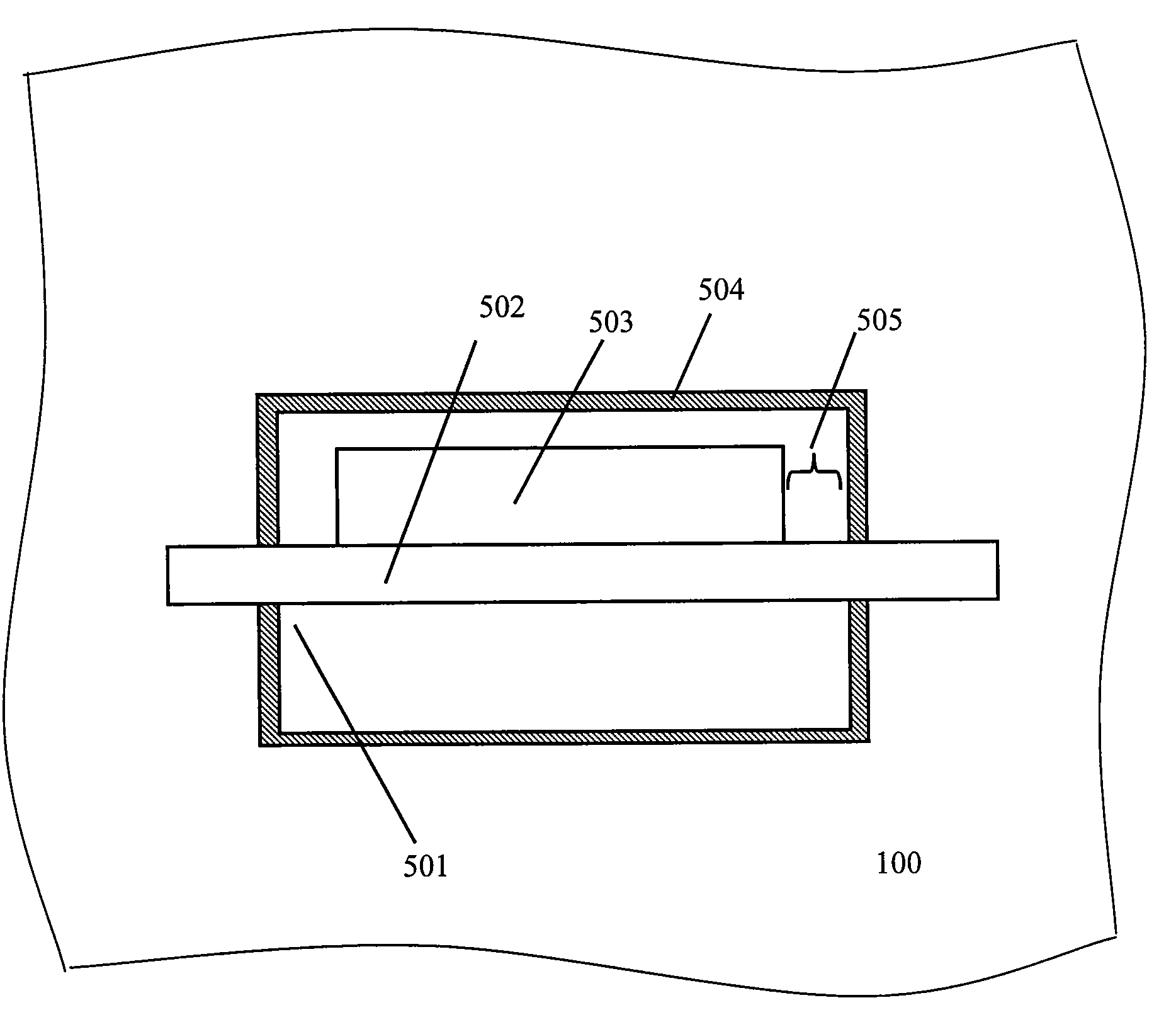
[0020]FIG. 1 is a schematic plan view showing an NMOS transistor for ESD protection of a semiconductor device according to a first embodiment of the present invention.
[0021]A pair of a source region 501 and a drain region 503 which are formed of an n-type heavily-doped impurity region are arranged on a p-type semiconductor substrate 100, a gate insulating film (not shown) made of a silicon oxide film or the like is placed between the source region 501 and the drain region 503, and a gate electrode 502 made of a polysilicon or the like is formed on an upper surface of the gate insulating film. A shallow trench structure is used for insulation from other elements, and a perimeter of the transistor is surrounded by a shallow trench isolation region 504. In this case, the drain region 503 is placed apart from the shallow trench isolation region 504, and a separation region 505 is formed between the drain region 503 and the shallow trench isolation region 504.
[0022]A region adjacent to t...
second embodiment
[0028]FIG. 2 is a schematic plan view showing an NMOS transistor for ESD protection of a semiconductor device according to a second embodiment of the present invention. The second embodiment is different from the first embodiment shown in FIG. 1 in that the separation region 505 placed between the drain region 503 and the shallow trench isolation region 504 is formed in a self-alignment manner in a region where the gate electrode 502 is extended.
[0029]In a generally-employed semiconductor manufacturing step, the gate electrode 502 is formed, and then the drain region 503 and the source region 501 are formed in a self-alignment manner with the gate electrode 502 using an ion implantation method or other methods in many cases. In the second embodiment shown in FIG. 2, in forming the drain region 503, the separation region 505 is automatically formed in the region where the gate electrode 502 is extended, with the result that the manufacturing step can be more simplified. Other parts a...
third embodiment
[0030]FIG. 3 is a schematic plan view showing an NMOS transistor for ESD protection of a semiconductor device according to a third embodiment of the present invention. The third embodiment is different from the first embodiment shown in FIG. 1 in that only regions of the drain region 503, which are adjacent to the gate electrode 502, are placed apart from the shallow trench isolation region 504.
[0031]A region of the NMOS transistor for ESD protection having the shallow trench isolation structure, where a largest amount of off leak current flows, is a channel region being adjacent to the shallow trench isolation region 504 and existing under the gate electrode 502. A junction between the drain region 503 in the vicinity of the shallow trench isolation region 504 and the p-type substrate 100 or a well region (not shown) is another part where the leak current is generated, but the leak current generated in the junction does not pose a serious problem in many cases.
[0032]The third embod...
PUM
 Abstract
Description
Claims
Application Information
 - R&D
- Intellectual Property
- Life Sciences
- Materials
- Tech Scout
- Unparalleled Data Quality
- Higher Quality Content
- 60% Fewer Hallucinations
Browse by: Latest US Patents, China's latest patents, Technical Efficacy Thesaurus, Application Domain, Technology Topic, Popular Technical Reports.
© 2025 PatSnap. All rights reserved.Legal|Privacy policy|Modern Slavery Act Transparency Statement|Sitemap|About US| Contact US: help@patsnap.com