Low voltage, master-slave flip-flop

a flip-flop and master-slave technology, applied in the field of low voltage master-slave flip-flop memory circuits, can solve the problems of power consumption increasing, circuits becoming more susceptible to thermal failure, etc., to achieve the effect of improving low voltage nominal hold and variability, without increasing circuit area or dynamic power consumption

Active Publication Date: 2019-09-05
STMICROELECTRONICS INT NV
View PDF1 Cites 0 Cited by
  • Summary
  • Abstract
  • Description
  • Claims
  • Application Information

AI Technical Summary

Benefits of technology

[0004]The present disclosure is directed to a transistor layout that improves low voltage nominal hold and variability in a master-slave flip-flop memory circuit without increasing circuit area or dynamic power consumption.
[0005]The present disclosure is directed to a master-slave flip-flop memory circuit with a re-architectured transistor layout that improves low voltage nominal hold and variability characteristics without increasing circuit area or dynamic power requirements. The circuit reduces the number of transistors in the nominal hold critical path by coupling an input of the master latch to a low output of the test switch around a partial pass gate. In addition, a first inverter is coupled to the input of the master latch with second and third inverters being coupled to an output of the first inverter. The second inverter has an output coupled to the input of the first inverter and the third inverter has an output coupled to an output of the master latch. The first and second inverters are clock enabled, and the third inverter is reset enabled, such that clock and reset signals are not inverted within the master latch.

Problems solved by technology

As switching speed increases, more current flows through the circuit and power consumption increases.
As power consumption increases, the circuit becomes more susceptible to thermal failure from the heat generated as power is dissipated by the circuit.
Thermal failure can result in erratic electrical signal behavior, spurious signals appearing in the circuit, or from component failure.
An unintended consequence of reduced source voltage is that transistor behavior can become more erratic as the threshold voltage of a transistor approaches the overall source voltage of the circuit.

Method used


Image

  • Low voltage, master-slave flip-flop
  • Low voltage, master-slave flip-flop
  • Low voltage, master-slave flip-flop

Examples


Embodiment Construction

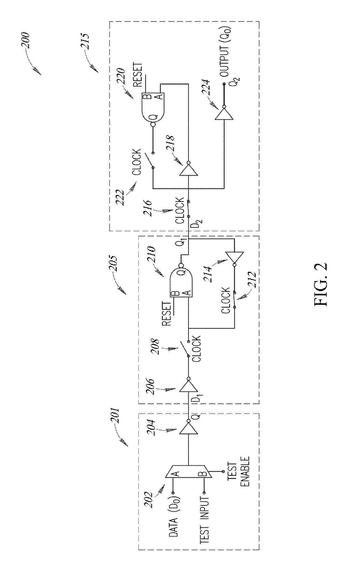
[0012]In the following description, certain specific details are set forth in order to provide a thorough understanding of various embodiments of the disclosure. However, one skilled in the art will understand that the disclosure may be practiced without these specific details. In other instances, well-known structures associated with electronic components and fabrication techniques have not been described in detail to avoid unnecessarily obscuring the descriptions of the embodiments of the present disclosure.

[0013]Unless the context requires otherwise, throughout the specification and claims that follow, the word “comprise” and variations thereof, such as “comprises” and “comprising,” are to be construed in an open, inclusive sense, that is, as “including, but not limited to.”

[0014]Reference throughout this specification to “one embodiment” or “an embodiment” means that a particular feature, structure or characteristic described in connection with the embodiment is included in at l...


PUM


Abstract

The present disclosure is directed to a master-slave flip-flop memory circuit having a partial pass gate transistor at the input of the master latch. The partial pass gate transistor includes a pull-up clock enabled transistor for selectively coupling a high output of a test switch to the input of the master latch. The input of the master latch is also directly coupled to a low output of the test switch around the partial pass gate. In addition, a revised circuit layout is provided in which the master latch has three inverters. A first inverter is coupled to the input of the master latch. Second and third inverters are coupled to an output of the first inverter, with the second inverter having an output coupled to the input of the first inverter, and the third inverter having an output coupled to an output of the master latch. The first and second inverters are clock enabled, and the third inverter is reset enabled.

Description

BACKGROUNDTechnical Field[0001]The present disclosure is directed to a master-slave flip-flop memory circuit, and in particular, to an arrangement of transistors to improve low voltage nominal hold and variability characteristics.Description of the Related Art[0002]Memory devices are common components in digital circuits. One type of memory is static random access memory (SRAM). SRAM cells use a latching circuit for each memory cell to preserve the data value over time without the use of a refreshing circuit. An output of a single D type latching circuit can be erratic during switching from the various inputs undergoing transitions. Thus one solution is to cascade two D type latches together. In this configuration, the first D type latch latches the desired value at a first time while the second D type latch continues to output a previously stored value. At a second time, the first D type latch outputs the previously received value to the second D type latch. This allows the inputs ...

Claims


Application Information

Patent Timeline
Patent Type & Authority Applications(United States)
IPC IPC(8): H03K3/3562G11C29/00
CPCH03K3/35625G11C11/412G11C29/00G11C16/30G11C29/48
Inventor TRIPATHI, ALOK KUMARVERMA, AMITGROVER, ANUJBIHANI, DEEPAK KUMARROY, TANMOYAGRAWAL, TANUJ
Owner STMICROELECTRONICS INT NV
Why Eureka
Try Eureka