Microdevices for high-throughput screening of biomolecules
a biomolecule and micro-device technology, applied in the field of micro-devices for high-throughput screening of biomolecules, can solve the problems of protein inactivation, volume less than 1 microliter in the well format, evaporation, dispensing time, etc., and achieve the effect of reducing reagent volume and protein inactivation problems
- Summary
- Abstract
- Description
- Claims
- Application Information
AI Technical Summary
Benefits of technology
Problems solved by technology
Method used
Image
Examples
example 1
Fabrication of a Microchannel Array by Bulk Micromachining
[0155]In a preferred embodiment microchannel arrays are fabricated via standard microstereolithography into the device material (bulk micromachining). Alternative techniques include surface-micromachining and LIGA (injection molding). Usually, a computer-aided design pattern (reflecting the final channel geometries) is transferred to a photomask using standard techniques, which is then used to transfer the pattern onto a silicon wafer coated with photoresist.
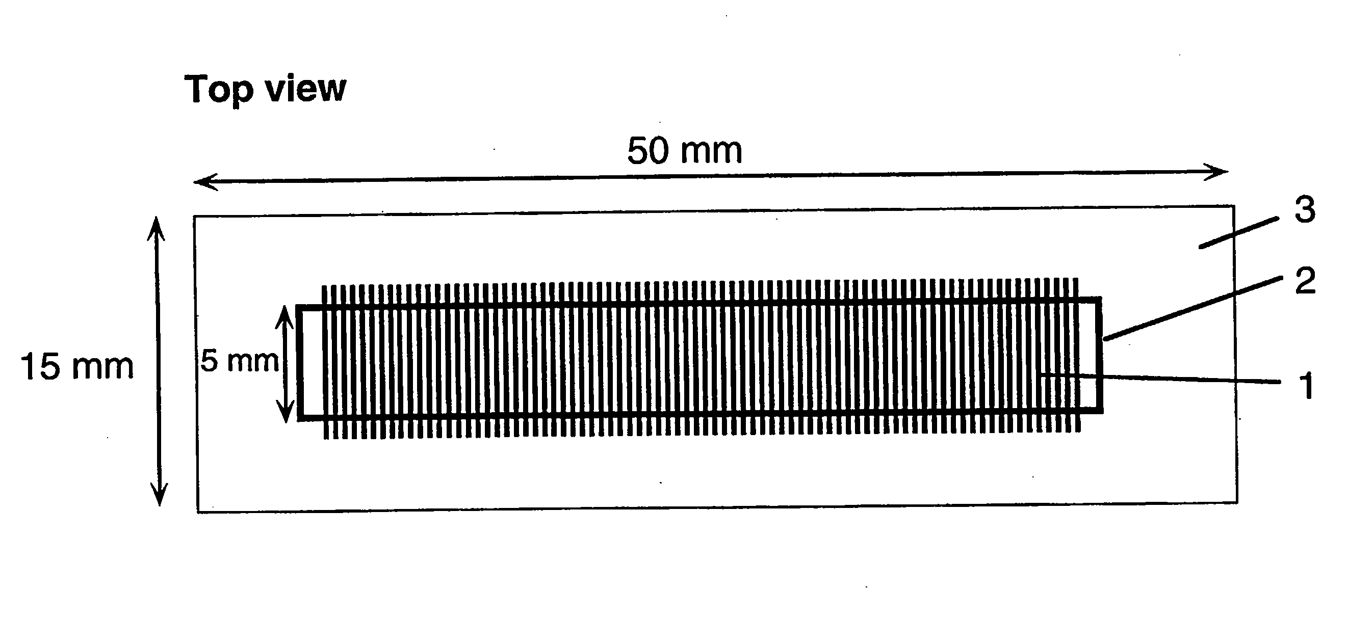
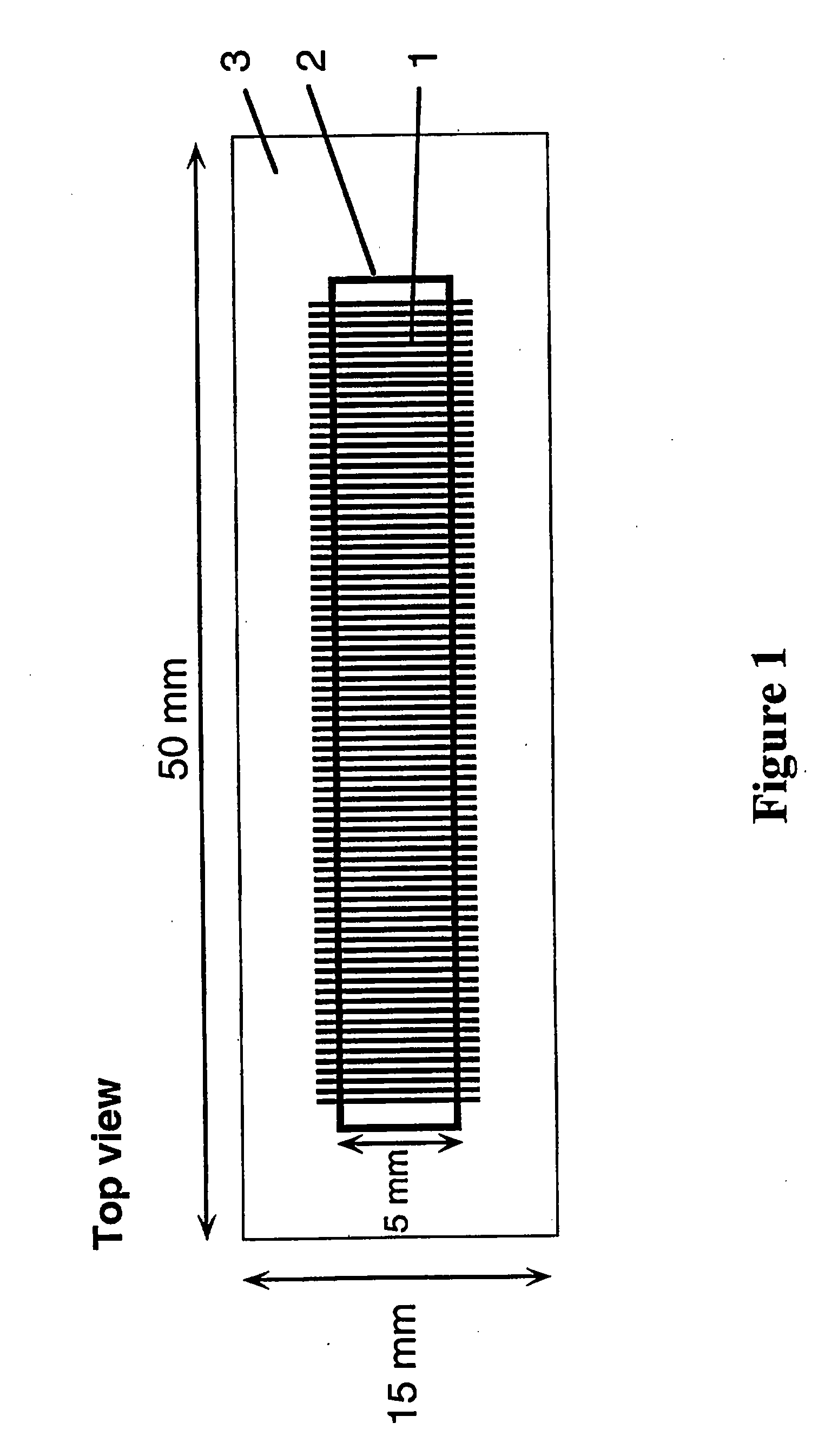
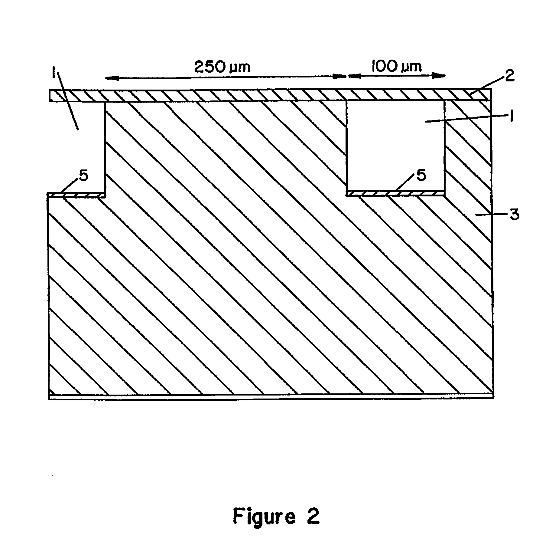
[0156]In a typical example, the device (“chip”), with lateral dimensions of 50×15 mm, contains a series of 100 parallel channels separated with a spacing of 250 μm. Each channel is 5 mm long and has a cross-section of 100×100 μm. The channel volume is 50 nl. 4″ diameter Si(100) wafers (Virginia Semiconductor) or 4″ diameter Corning 7740 glass wafers are used as bulk materials. Si(100) wafers are first cleaned in a 5:1:1 DI water:NH3:H2O2 bath (RCA1, 90° C., 10 min), follo...
example 2
Fabrication of a Microchannel Array by Sacrificial Micromachining
[0158]In sacrificial micromachining, the bulk material is left essentially untouched. Various thick layers of other materials are built up by either physical vapor deposition (PVD), plasma-enhanced chemical vapor deposition (PECVD) or spin coating and selectively remain behind or are removed by subsequent processing steps. Thus, the resulting channel walls are chemically different from the bottom of the channels and the resist material remains as part of the microdevice. Typical resist materials for sacrificial micromachining are silicon nitride (Si3N4), polysilicon, thermally grown silicon oxide and organic resists such as epoxy-based SU-8 and polyimides allowing the formation of high aspect-ratio features with straight sidewalls.
[0159]In a typical example, the device (“chip”), with lateral dimensions of 50×15 mm, contains a series of 100 parallel channels separated with a spacing of 250 μm. Each channel is 5 mm long ...
example 3
Synthesis of an Aminoreactive Monolayer Molecule (Following the Procedure Outlined in Wagner et al., Biophys. J., 1996, 70:2052-2066)
[0161]General. 1H- and 13C-NMR spectra are recorded on Bruker instruments (100 to 400 MHz). Chemical shifts (δ) are reported in ppm relative to internal standard ((CH3)4Si, δ=0.00 (1H- and 13C-NMR)). FAB-mass spectra are recorded on a VG-SABSEQ instrument (Cs+, 20 keV). Transmission infrared spectra are obtained as dispersions in KBr on an FTIR Perkin-Elmer 1600 Series instrument. Tin-layer chromatography (TLC) is performed on precoated silica gel 60 F254 plates (MERCK, Darmstadt, FRG), and detection was done using Cl2 / toluidine, PdCl2 and UV-detection under NH3-vapor. Medium pressure liquid chromatography (MPLC) is performed on a Labomatic MD-80 (LABOMATIC INSTR. AG, Allschwil, Switzerland) using a Buechi column (460×36 mm; BUECHI, Flawil, Switzerland), filled with silica gel 60 (particle size 15-40 μm) from Merck.
[0162]Synthesis of 11,11′-dithiobis(s...
PUM
| Property | Measurement | Unit |
|---|---|---|
| distance | aaaaa | aaaaa |
| distance | aaaaa | aaaaa |
| width | aaaaa | aaaaa |
Abstract
Description
Claims
Application Information
 - R&D Engineer
- R&D Manager
- IP Professional
- Industry Leading Data Capabilities
- Powerful AI technology
- Patent DNA Extraction
Browse by: Latest US Patents, China's latest patents, Technical Efficacy Thesaurus, Application Domain, Technology Topic, Popular Technical Reports.
© 2024 PatSnap. All rights reserved.Legal|Privacy policy|Modern Slavery Act Transparency Statement|Sitemap|About US| Contact US: help@patsnap.com


