
Metallic compound hybridized nanophosphor layer, applications thereof, and method of preparing a metallic compound hybridized nanophosphor layer

a technology of nanophosphor and compound, applied in the direction of discharge tube/lamp details, discharge tube luminescnet screen, gas-filled discharge tube, etc., can solve the problems of nanophosphor particle surface chemical degradation, decrease in phosphor characteristics, surface defects, etc., and achieve excellent phosphor layer properties.

Inactive Publication Date: 2009-01-08
SAMSUNG SDI CO LTD
View PDF7 Cites 26 Cited by
  • Summary
  • Abstract
  • Description
  • Claims
  • Application Information

AI Technical Summary

Benefits of technology

[0011]The present invention provides a metallic compound hybridized nanophosphor layer having excellent properties prepared in consideration of physical, mechanical, chemical stabilities.
[0025]The metallic compound hybridized nanophosphor layer according to the present invention is prepared in consideration of physical, mechanical, chemical stabilities to obtain excellent phosphor layer properties. Thus, the metallic compound hybridized nanophosphor layer is suitable for various display devices. In addition, the method of forming a metallic compound hybridized nanophosphor layer according to the present invention can provide a metallic compound hybridized nanophosphor layer having physical, mechanical, and chemical stabilities in mild conditions.

Problems solved by technology

However, when the conventional method is used with nanophosphor which has a small particle size and a large specific surface area, surface defects may occur due to high temperature heat treatment, and chemical degradation may occur at the surface of nanophosphor particles.
These problems may lead to a decrease in phosphor characteristics and further, loss of phosphor characteristics.
When a nanophosphor layer prepared using the conventional method is used in display devices, optical properties and physical and chemical stabilities such as stability with respect to ion-bombardment and thermal stability, cannot be obtained.
Thus, such a nanophosphor is unsuitable for operation methods of a display.
Specifically, plasma display panels (PDPs) require durability against ion bombardment and a function to be able to remove a charging effect, but such a nanophosphor does not comply with the requirements described above.

Method used


Image

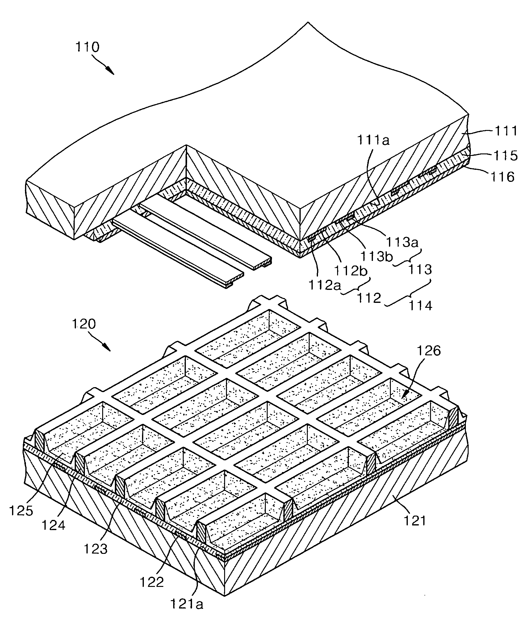
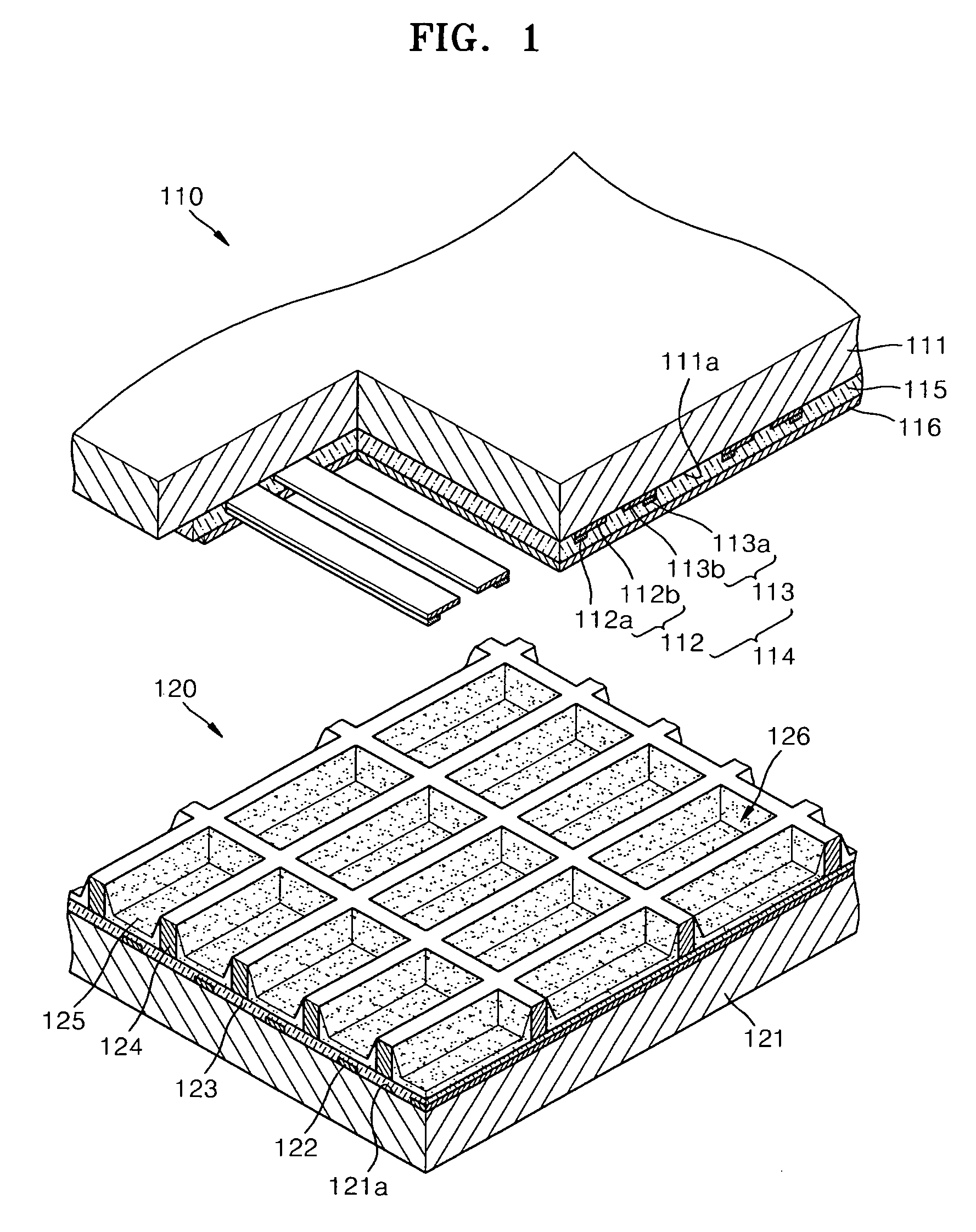
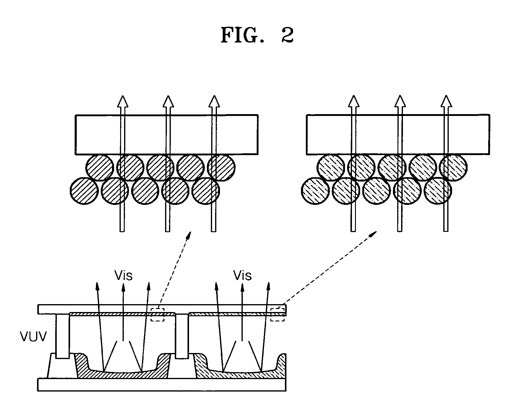
  • Metallic compound hybridized nanophosphor layer, applications thereof, and method of preparing a metallic compound hybridized nanophosphor layer
  • Metallic compound hybridized nanophosphor layer, applications thereof, and method of preparing a metallic compound hybridized nanophosphor layer
  • Metallic compound hybridized nanophosphor layer, applications thereof, and method of preparing a metallic compound hybridized nanophosphor layer

Examples


example 1

[0089]YBO3:Eu nanophosphor was used as a phosphor. A nanophosphor layer was formed by performing a wetting process at room temperature and atmospheric pressure.

[0090]Then, a glass substrate on which the nanophosphor layer was formed was immersed in a methanol solution in which the concentration of Mg2+-containing salt dissolved was 0.05 N for 15 minutes, thereby allowing Mg2+ to permeate between the nanophosphor particles. Alternatively, Mg2+-containing solution can be mixed with the nanophosphor particles and may be casted on the substrate surface. Then, the resultant product was treated with an NH4OH aqueous solution so that the permeated Mg2+ was converted to MgO / Mg(OH)2 between the nanophosphor particles. Mg(OH)2 was converted into MgO by performing a heat treatment at 300° C. in a vacuum condition which is higher than a transition temperature. As a result, a MgO:YBO3:Eu nanophosphor hybrid layer was formed.

example 2

[0091]The same method as described in Example 1 was used using Zn2+-containing salt instead of Mg2+-containing salt, so that ZnO / Zn(OH)2 was formed between nanophosphor particles. Then, Zn(OH)2 was converted into ZnO by performing a heat treatment process at 125° C. which is at or higher than a transition temperature. As a result, a ZnO:YBO3:Eu nanophosphor hybrid layer was formed.

example 3

[0092]The same method as described in Example 1 was used using La3+-containing salt instead of Mg2+-containing salt, so that La2O3 / La(OH)3 was formed between nanophosphor particles. Then, La(OH)3 was converted into La2O3 by performing a heat treatment process at 340° C. which is at or higher than a transition temperature. As a result, a La2O3:YBO3:Eu nanophosphor hybrid layer was formed.


PUM


Abstract

A metallic compound hybridized nanophosphor layer, in which the metallic compound is metallic oxide or metallic sulfide. The metallic compound hybridized nanophosphor layer is prepared in consideration of physical, mechanical, and chemical stabilities. The metallic compound hybridized nanophosphor layer has an excellent light scattering effect and high durability against damage from ion-bombardment. In addition, the charging effect caused by V-UV vacuum-ultraviolet ray can be considerably reduced. Thus, the metallic compound hybridized nanophosphor layer is very suitable for various display devices having high efficiency and high resolution. Accordingly, a display device using the metallic compound hybridized nanophosphor layer shows high performance and long lifetime. The method of forming the metallic compound hybridized nanophosphor layer is a low temperature layer forming process through which a thin film-type layer can be formed at low temperature. Therefore, a phosphor layer having physical, mechanical, and chemical stabilities can be formed at low cost.

Description

CROSS-REFERENCE TO RELATED PATENT APPLICATIONS AND CLAIM OF PRIORITY[0001]This application claims the benefit of Korean Patent Application No. 10-2007-0068181, filed on Jul. 6, 2007, in the Korean Intellectual Property Office, the disclosure of which is incorporated herein in its entirety by reference.BACKGROUND OF THE INVENTION[0002]1. Field of the Invention[0003]The present invention relates to a nanophosphor film hybridized with metallic compounds in which the metallic compound is metallic oxide or metallic sulfide, applications thereof, and a method of preparing a metallic compound hybridized nanophosphor layer.[0004]2. Description of the Related Art[0005]Phosphor is a substance that exhibits the phenomenon of fluorescence / phosphorescence (short / sustained glowing after exposure to oxygen or energized particles such as electrons, or lights such as ultraviolet / vacuum-ultraviolet / visible light). In general, a phosphor is used in light sources such as Hg (mercury) phosphor lamps or ...

Claims


Application Information

Patent Timeline
IPC IPC(8): H01J1/62B05D5/12B82Y20/00C09K11/00C09K11/08C09K11/54C09K11/58C09K11/59C09K11/62C09K11/64C09K11/78C09K11/80C09K11/81C09K11/83H01J11/10H01J11/12H01J11/36H01J11/42H05B33/14
CPCC09K11/7797H05B33/145H01J11/42H01J11/12C09K11/08C09K11/56B82B3/00
Inventor KWON, SOON-JAEKIM, HYUN-SIK
Owner SAMSUNG SDI CO LTD
Learn More