Heat spreader and method for manufacturing the same, and semiconductor device
a technology of heat spreader and semiconductor device, which is applied in the direction of semiconductor/solid-state device details, electrical apparatus construction details, transportation and packaging, etc., can solve the problems of difficult to provide the semiconductor device with such high reliability, easy oxidation and corrosion of exposed cu, and plating layer, etc., to achieve good reproducibility and efficient
- Summary
- Abstract
- Description
- Claims
- Application Information
AI Technical Summary
Benefits of technology
Problems solved by technology
Method used
Image
Examples
example 1
Production of Base Substrate
[0102]1% by mass of an acrylic binder was added to W powder having an average particle diameter of 3 μm, to granulate the powder to obtain a granulated body having an average particle diameter of 50 μm. A recess, whose plane shape was a rectangle having dimensions of 30 mm in width by 110 mm in length, of a metal mold was filled with the granulated body, and the granulated body was press-molded to the shape of a rectangular plane under a surface pressure of 1.5 ton / cm2, and was then heated for one hour at a temperature of 800° C. in a hydrogen gas atmosphere to remove the binder, and was then successively heated to 1250° C. in the hydrogen gas atmosphere and was sintered, to produce a porous body composed of W.
[0103]The porous body was then heated to 1250° C. in the hydrogen gas atmosphere, with the porous body overlapped with a Cu plate whose volume was 1.3 times of the porosity of the porous body, to dissolve Cu, to infiltrate the Cu into pores of the p...
example 2
Comparative Examples 2 and 3
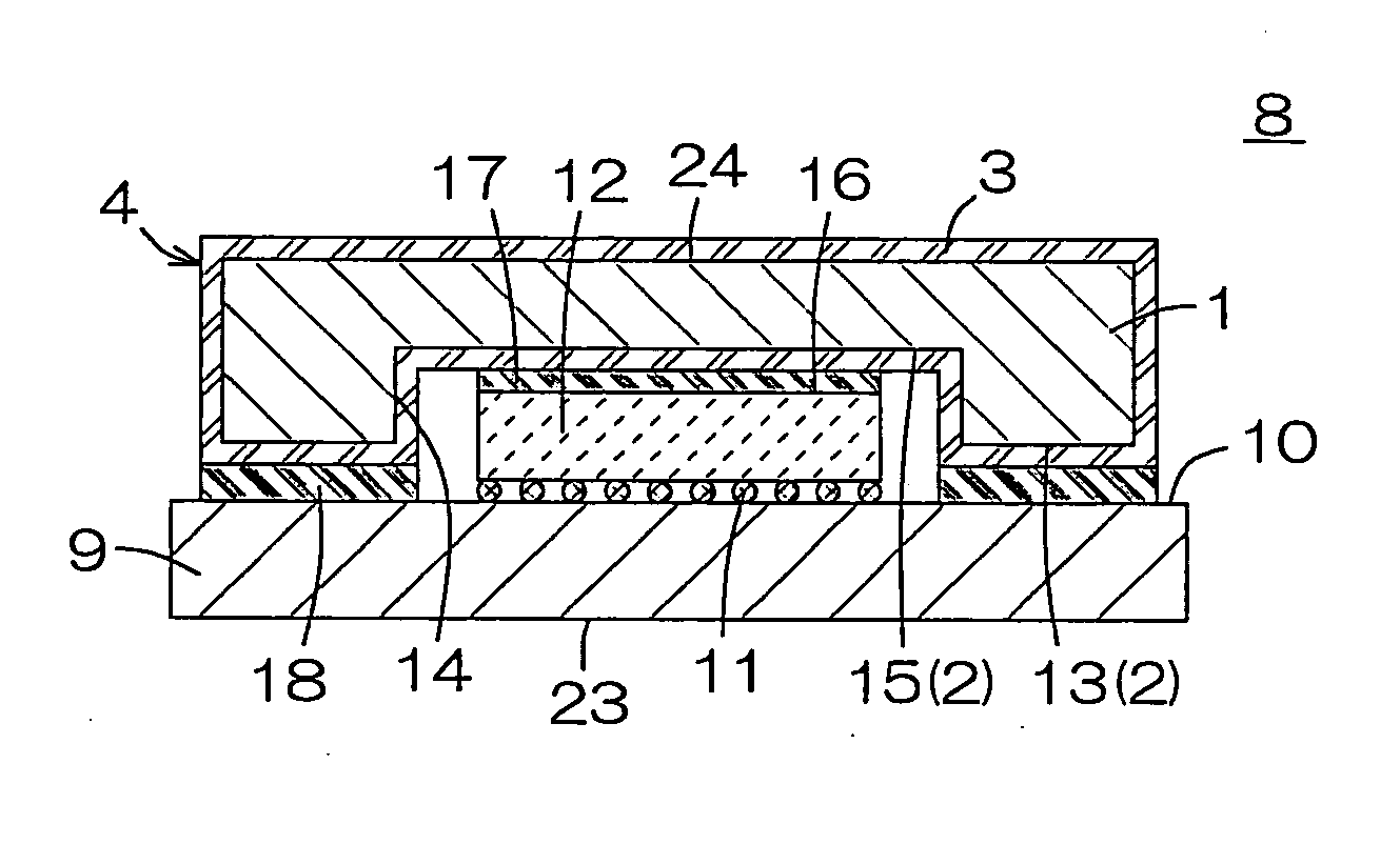
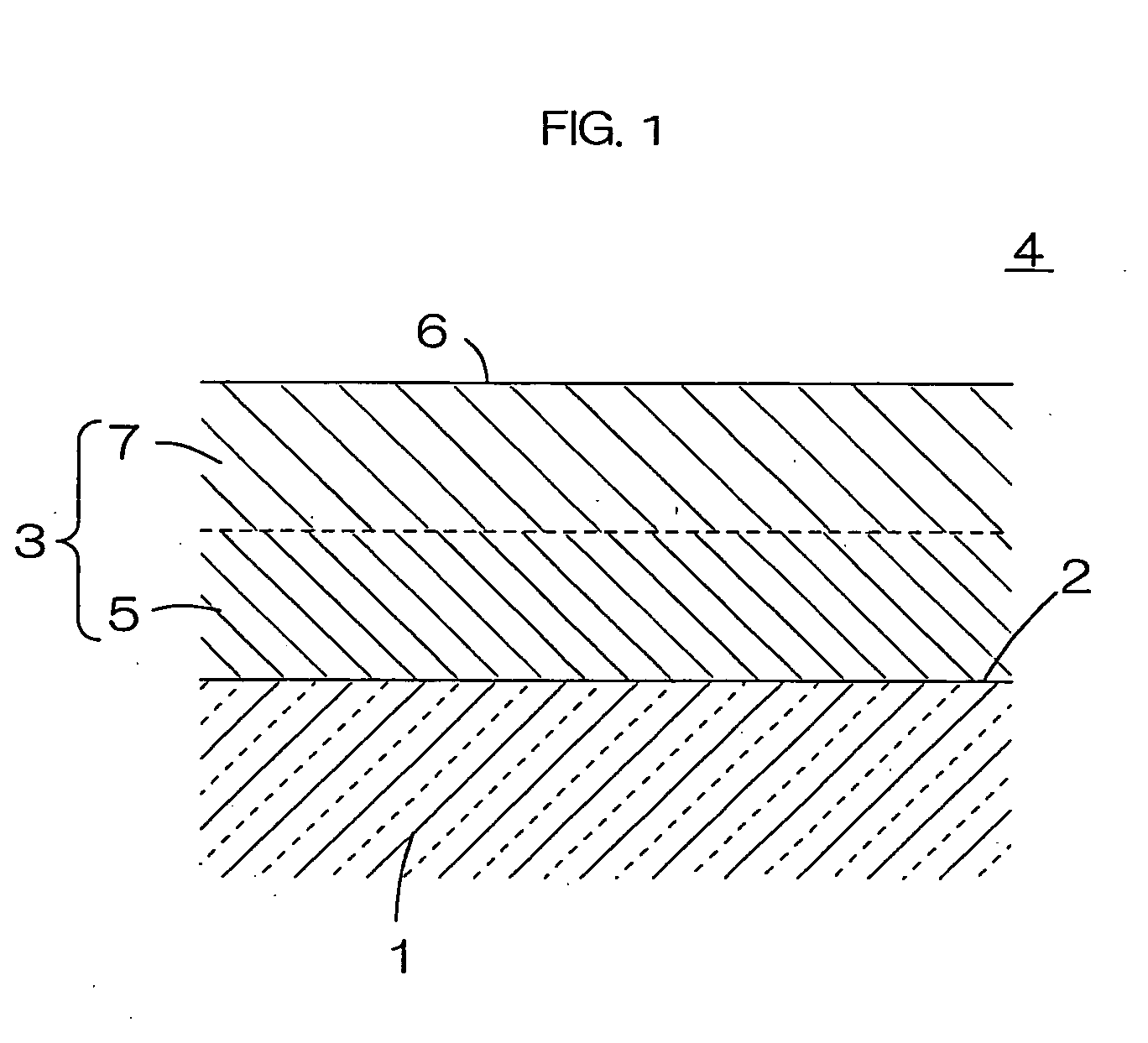
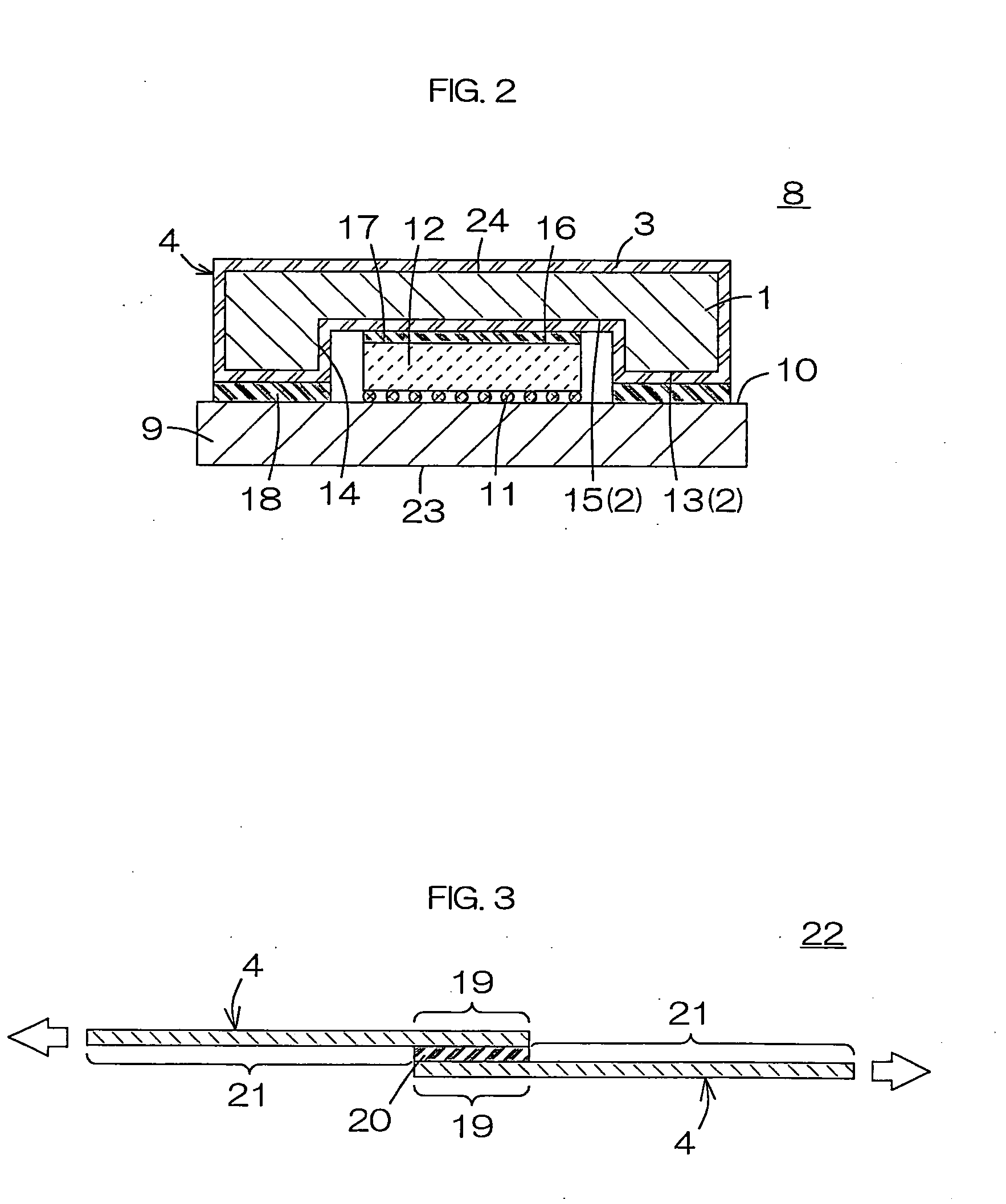
[0117]Heat spreaders were manufactured in the same manner as that in the example 1 except that the thickness of a first plating layer was 0.05 μm (comparative example 2), 0.2 μm (example 2), and 2.1 μm (comparative example 3).
examples 3 and 4
Comparative Example 4
[0118]Heat spreaders were manufactured in the same manner as that in the example 1 except that the thickness of a second plating layer was 0.3 μm (comparative example 4), 0.6 μm (example 3), and 2.5 μm (example 4).
PUM
| Property | Measurement | Unit |
|---|---|---|
| Temperature | aaaaa | aaaaa |
| Length | aaaaa | aaaaa |
| Percent by mass | aaaaa | aaaaa |
Abstract
Description
Claims
Application Information
 - R&D
- Intellectual Property
- Life Sciences
- Materials
- Tech Scout
- Unparalleled Data Quality
- Higher Quality Content
- 60% Fewer Hallucinations
Browse by: Latest US Patents, China's latest patents, Technical Efficacy Thesaurus, Application Domain, Technology Topic, Popular Technical Reports.
© 2025 PatSnap. All rights reserved.Legal|Privacy policy|Modern Slavery Act Transparency Statement|Sitemap|About US| Contact US: help@patsnap.com


