Optical Recording Medium
a recording medium and optical technology, applied in the field of optical recording mediums, can solve the problems of insufficient recording and reproducing characteristics, high cost, and inability to use the reflective layer for optical recording devices
- Summary
- Abstract
- Description
- Claims
- Application Information
AI Technical Summary
Benefits of technology
Problems solved by technology
Method used
Image
Examples
example 1
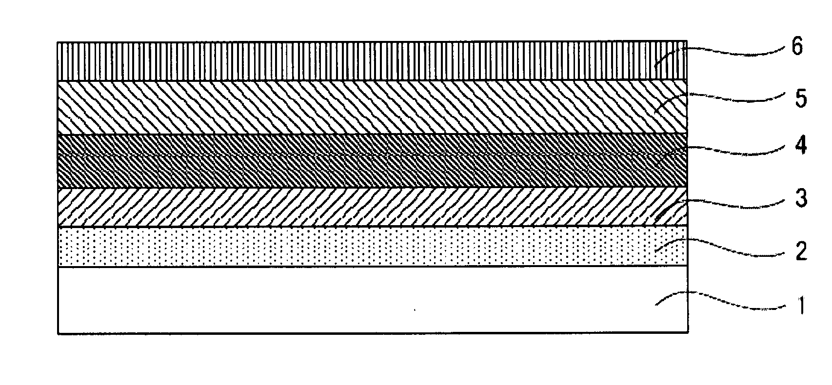
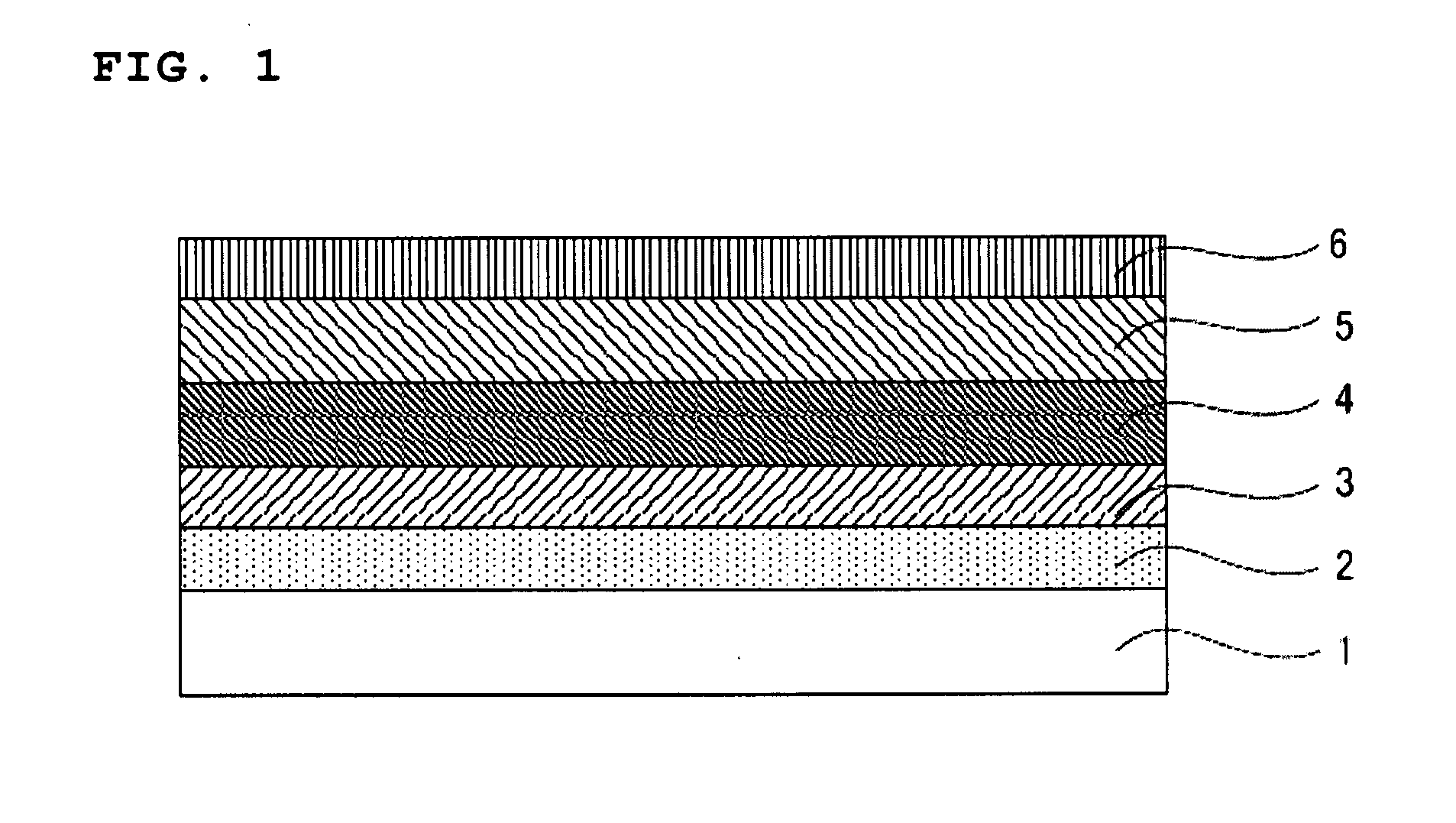
[0051]On an amorphous polyolefin disc substrate with 1.1 mm thickness, 12 cm diameter and 0.320 μm pitch spiral groove, a reflective layer (Al—Pd—SnO2), a dielectric protective layer (Nb—Si—O—N), a recording layer (Bi—Ge—N) and a second dielectric protective layer (Nb—Si—O—N) were deposited in this order by the sputtering process. The thickness of each one were 50 nm, 30 nm, 15 nm and 24 nm respectively. Thereinafter, as an incident side substrate (cover layer), a 0.1 mm thickness ultraviolet curable resin layer was laminated onto the second dielectric protective layer.
[0052]Here, the reflective layer is a layer obtained by sputtering in argon (Ar) atmosphere of 0.2 Pa using a sputtering target where 2.0% by weight of tin dioxide (SnO2) was added to an aluminum alloy of aluminum and palladium.
[0053]According to analysis with an inductively-coupled plasma atomic emission spectrometry (ICP-AES) of the reflective layer, palladium (Pd) was contained in the aluminum by about 4 atm %, and...
examples 2 to 12
[0059]An optical recording medium was produced in the same manner as in the example 1 except that polycarbonate (PC) was used for the substrate, a polycarbonate (PC) sheet laminated with a ultraviolet curable resin was used for the cover layer, and the thicknesses of the dielectric protective layer, recording layer and second dielectric protective layer were changed as shown in the table 1.
(Evaluation)
[0060]According to the measurement of the jitter value in the same manner as in the example 1, as shown in the table 1, a preferable jitter value was obtained in any case, and it shows sufficient practical use.
TABLE 1SecondDielectricdielectricReflectiveprotectiveRecordingprotectiveCoverSubstratelayerlayerlayerlayerlayerJitterPCAl—Pd—SnO2Nb—Si—O—NBi—Ge—NNb—Si—O—NPCvalueExample 21.1 mm50 nm28 nm12 nm25 nm0.1 mm7.1Example 31.1 mm50 nm30 nm12 nm25 nm0.1 mm6.9Example 41.1 mm50 nm36 nm12 nm25 nm0.1 mm7.1Example 51.1 mm50 nm30 nm12 nm15 nm0.1 mm7.1Example 61.1 mm50 nm20 nm12 nm30 nm0.1 mm7.9E...
examples 13 to 16
[0061]An optical recording medium was produced in the same manner as in the example 1 except that polycarbonate (PC) was used for the substrate, a polycarbonate (PC) sheet laminated with a ultraviolet curable resin was used for the cover layer, and the second dielectric protective layer was a layer containing as the main component a niobium composition containing titanium oxide and niobium nitrided oxide (Nb—Ti—O—N) with the thicknesses as shown in the table 2.
[0062]The second dielectric protective layer is a layer obtained by sputtering in Ar+N2 (5%) atmosphere of 0.37 Pa using a sputtering target of Nb2O3—TiO2 (TiO2: 96% by weight).
[0063]According to the measurement of the jitter value in the same manner as in the example 1, as shown in the table 2, a preferable jitter value was obtained in any case, and it shows sufficient practical use.
TABLE 2SecondDielectricdielectricReflectiveprotectiveRecordingprotectiveCoverSubstratelayerlayerlayerlayerlayerJitterPCAl—Pd—SnO2Nb—Si—O—NBi—Ge—N...
PUM
| Property | Measurement | Unit |
|---|---|---|
| particle size | aaaaa | aaaaa |
| thickness | aaaaa | aaaaa |
| diameter | aaaaa | aaaaa |
Abstract
Description
Claims
Application Information
 - R&D
- Intellectual Property
- Life Sciences
- Materials
- Tech Scout
- Unparalleled Data Quality
- Higher Quality Content
- 60% Fewer Hallucinations
Browse by: Latest US Patents, China's latest patents, Technical Efficacy Thesaurus, Application Domain, Technology Topic, Popular Technical Reports.
© 2025 PatSnap. All rights reserved.Legal|Privacy policy|Modern Slavery Act Transparency Statement|Sitemap|About US| Contact US: help@patsnap.com


