Large grain, multi-crystalline semiconductor ingot formation method and system

Inactive Publication Date: 2008-10-23
SILICOR MATERIALS INC
View PDF8 Cites 31 Cited by
  • Summary
  • Abstract
  • Description
  • Claims
  • Application Information

AI Technical Summary

Benefits of technology

[0008]Techniques are here disclosed for providing a combination of interrelated steps at the ingot formation level for ultimately making economically viable the fabrication of solar cells on a mass production level. The present disclosure includes a method and system for forming multicrystalline silicon ingots, which ingots include large grain sizes. With the disclosed process and system silicon ingots may formed directly within a silicon melt crucible. The disclosed process forms a large-grain multi-crystalline ingot from molten silicon by precisely controlling local crystallization temperatures throughout a process crucible. The process operates on the molten silicon and uses the driving force inherent to the transition from the liquid state to the solid state as the force which drives the grain growth process. For example, using multicrystalline silicon ingots formed from the processes here disclosed, solar wafers and solar cells, based on this multicrystalline material, with improved performance / cost ratio are practical. In addition, the present disclosure may readily and efficiently combine with metal-related defect engineering at the wafer level to yield a highly efficient PV solar cell.

Problems solved by technology

EG silicon yields solar cells having efficiencies close to the theoretical limit, but at a prohibitive price.
On the other hand, MG silicon typically fails to produce working solar cells.
Because of the high cost and complex processing requirements of obtaining and using highly pure silicon feedstock and the competing demand from the IC industry, silicon needs usable for solar cells are not likely to be satisfied by either EG, MG, or other silicon producers using known processing techniques.
As long as this unsatisfactory situation persists, economical solar cells for large-scale electrical energy production may not be attainable.
Accordingly, a need exists for a source of silicon ingots to meet the silicon needs of the solar cell industry, which source may not compete with the demands of the IC industry.

Method used


Image

  • Large grain, multi-crystalline semiconductor ingot formation method and system
  • Large grain, multi-crystalline semiconductor ingot formation method and system
  • Large grain, multi-crystalline semiconductor ingot formation method and system

Examples


embodiment 150

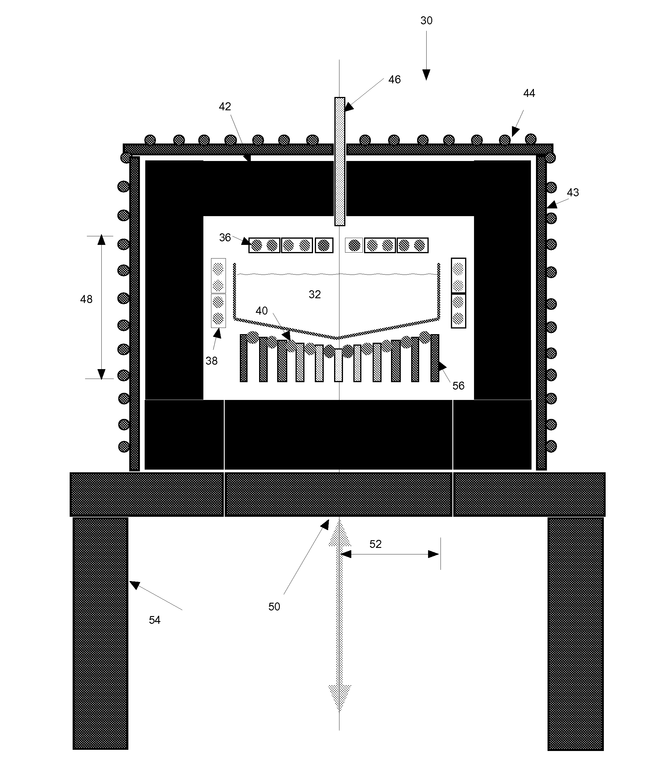
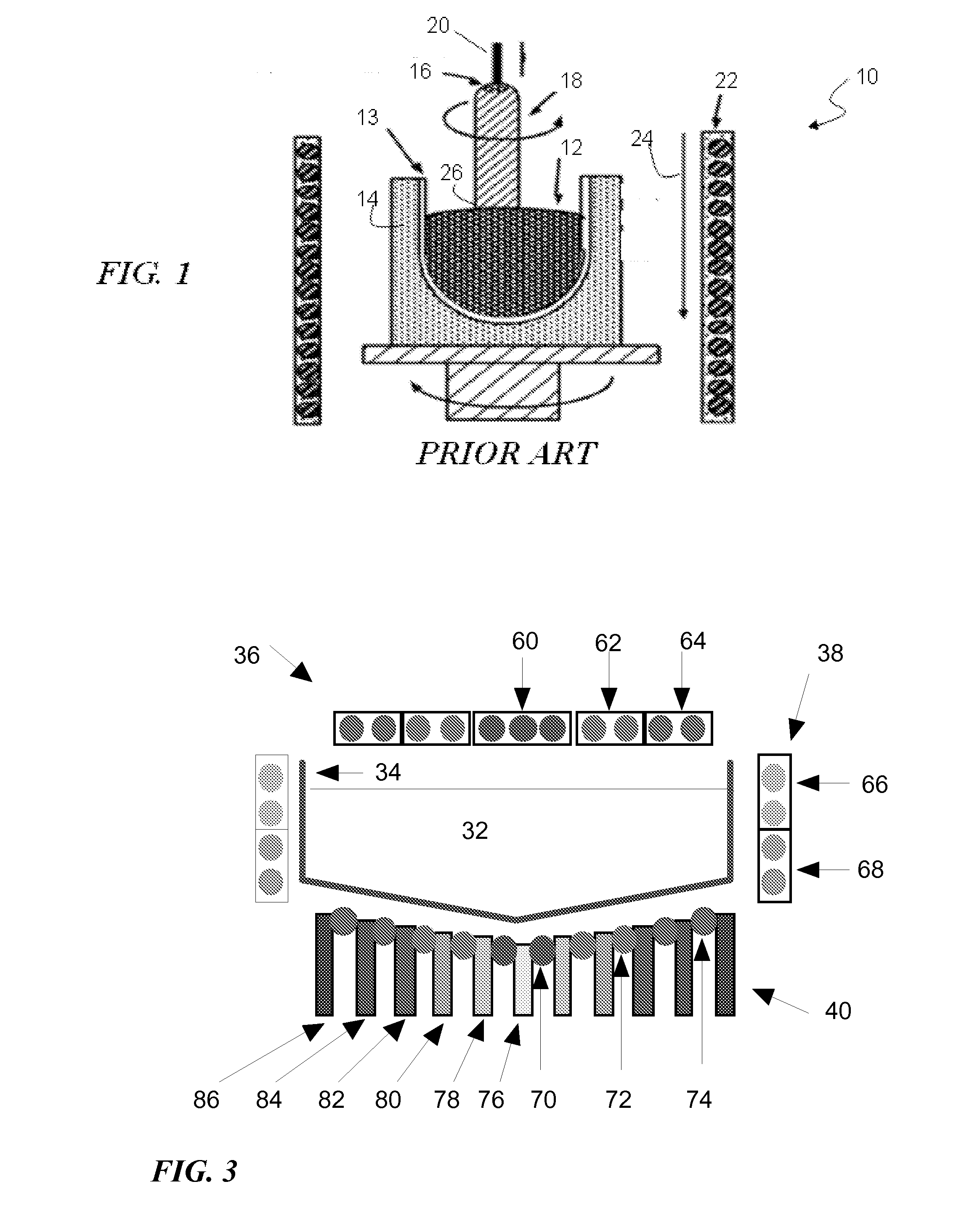
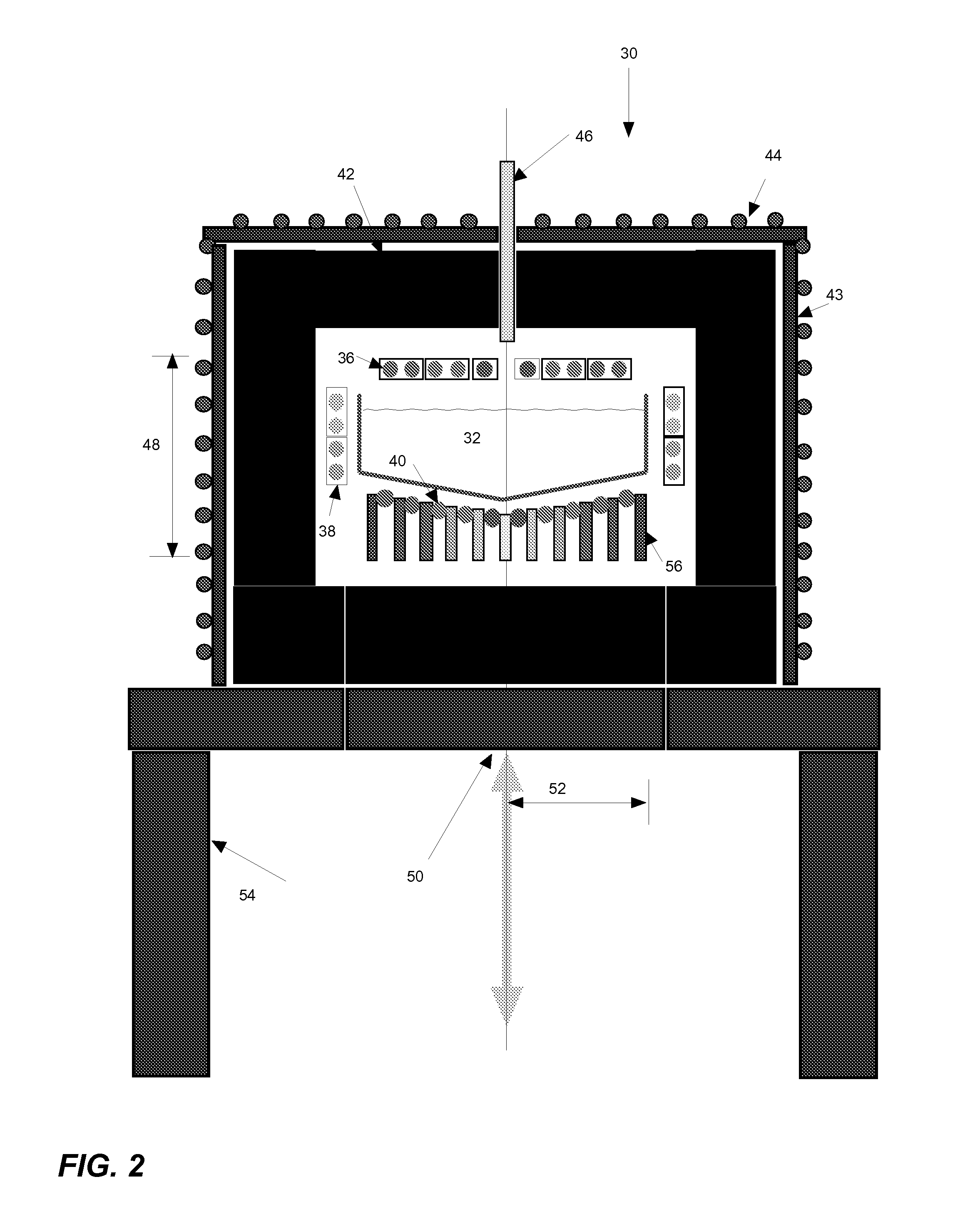
[0037]As with the above-described process environments, process environment 150 may include a set of lower heating elements 162. Lower heating elements 162 may include individually controllable heaters 164 through 174 for managing temperatures, mixing and solidification of silicon melt 32, while accommodating the various control features and concerns relating to the non-symmetrical nature of modified crucible 152. Embodiment 150 may include upper heating elements as shown in FIGS. 2, 3, 5 and 7, aligned on the crucible shape and the process environment.

[0038]For a more clear view of modified 152, FIG. 9 shows an isometric perspective wherein below line or plane 155 appears slanted bottom 154. Bottom 154, due to the slant forms a process control volume 156 wherein silicon crystallization may initially occur. Heating element 160, therefore, provides process temperature control for process control volume 156. Within process control volume 156 silicon crystallization may initially occur...

embodiment 180

[0039]FIG. 10 shows an embodiment 180 for a direct solidification of a silicon melt using a seed crystal to get a monocrystalline silicon ingot or a multicrystalline ingot with large grain sizes and a lower number of grains for a given volume. In particular, seed crystal 33 may be positioned at the bottom of crucible 34, which may include all of the various forms and shapes of crucibles herein disclosed. Moreover, using the local and precise silicon crystallization techniques here disclosed, the combination of a seed crystal may further enhance the growth of large grain sizes and, consequently, is within the scope of the present disclosure.

[0040]The present disclosure, therefore, provides a multi-crystalline silicon ingot with a preferably low number of big grains. Using the presently disclosed fabrication system, silicon melt 32 may be cooled-beginning from the center of crucible 34—using an Argon or helium flow and the programmably controlled heating elements 40. This translates t...


PUM


Abstract

Techniques for the formation of a large grain, multi-crystalline semiconductor ingot and include forming a silicon melt in a crucible, the crucible capable of locally controlling thermal gradients within the silicon melt. The local control of thermal gradients preferentially forms silicon crystals in predetermined regions within the silicon melt by locally reducing temperatures is the predetermined regions. The method and system control the rate at which the silicon crystals form using local control of thermal gradients for inducing the silicon crystals to obtain preferentially maximal sizes and, thereby, reducing the number of grains for a given volume. The process continues the thermal gradient control and the rate control step to form a multicrystalline silicon ingot having reduced numbers of grains for a given volume of the silicon ingot.

Description

FIELD[0001]The present disclosure relates to methods and systems for use in the fabrication of semiconductor materials such as silicon. More particularly, the present disclosure relates to large grain, multi-crystalline semiconductor ingot formation method and system for producing a high purity semiconductor ingot.DESCRIPTION OF THE RELATED ART[0002]The photovoltaic industry (PV) industry is growing rapidly and is responsible for increasing industrial consumption of silicon being consumed beyond the more traditional integrated circuit (IC) applications. Today, the silicon needs of the solar cell industry are starting to compete with the silicon needs of the IC industry. With present manufacturing technologies, both integrated circuit (IC) and solar cell industries require a refined, purified, silicon feedstock as a starting material.[0003]Materials alternatives for solar cells range from single-crystal, electronic-grade (EG) silicon to relatively dirty, metallurgical-grade (MG) sili...

Claims


Application Information

Patent Timeline
IPC IPC(8): C30B15/20
CPCC01B33/037C30B11/002C30B11/003Y10T117/1008C30B29/06H01L31/1804Y02E10/547C30B28/06Y02P70/50
Inventor LINKE, DIETERHEUER, MATTHIASKIRSCHT, FRITZRAKOTONIANA, JEAN PATRICEOUNADJELA, KAMEL
Owner SILICOR MATERIALS INC
Why Eureka
Try Eureka