Wiring structure of semiconductor integrated circuit device, and method and device for designing the same
- Summary
- Abstract
- Description
- Claims
- Application Information
AI Technical Summary
Benefits of technology
Problems solved by technology
Method used
Image

Examples
first embodiment
[0096]Hereinafter, a method and device for designing a wiring structure according to a first embodiment of the present invention, and a wiring structure obtained by the designing method and device, will be described.
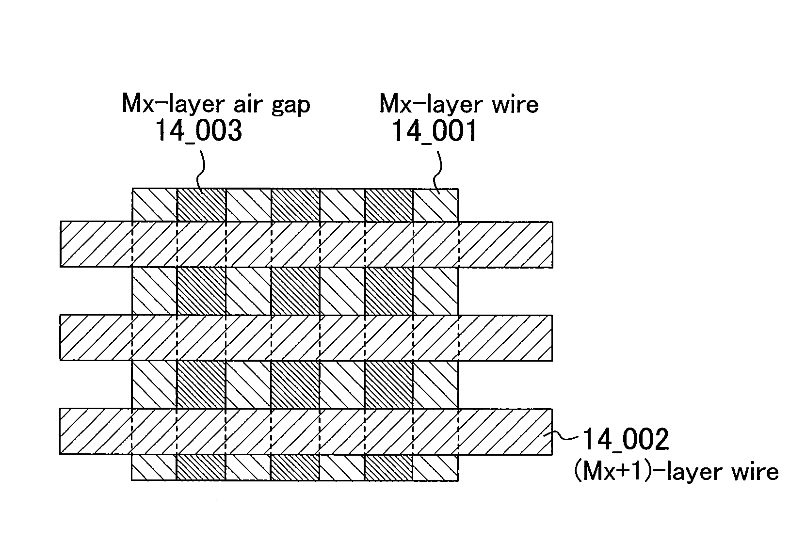
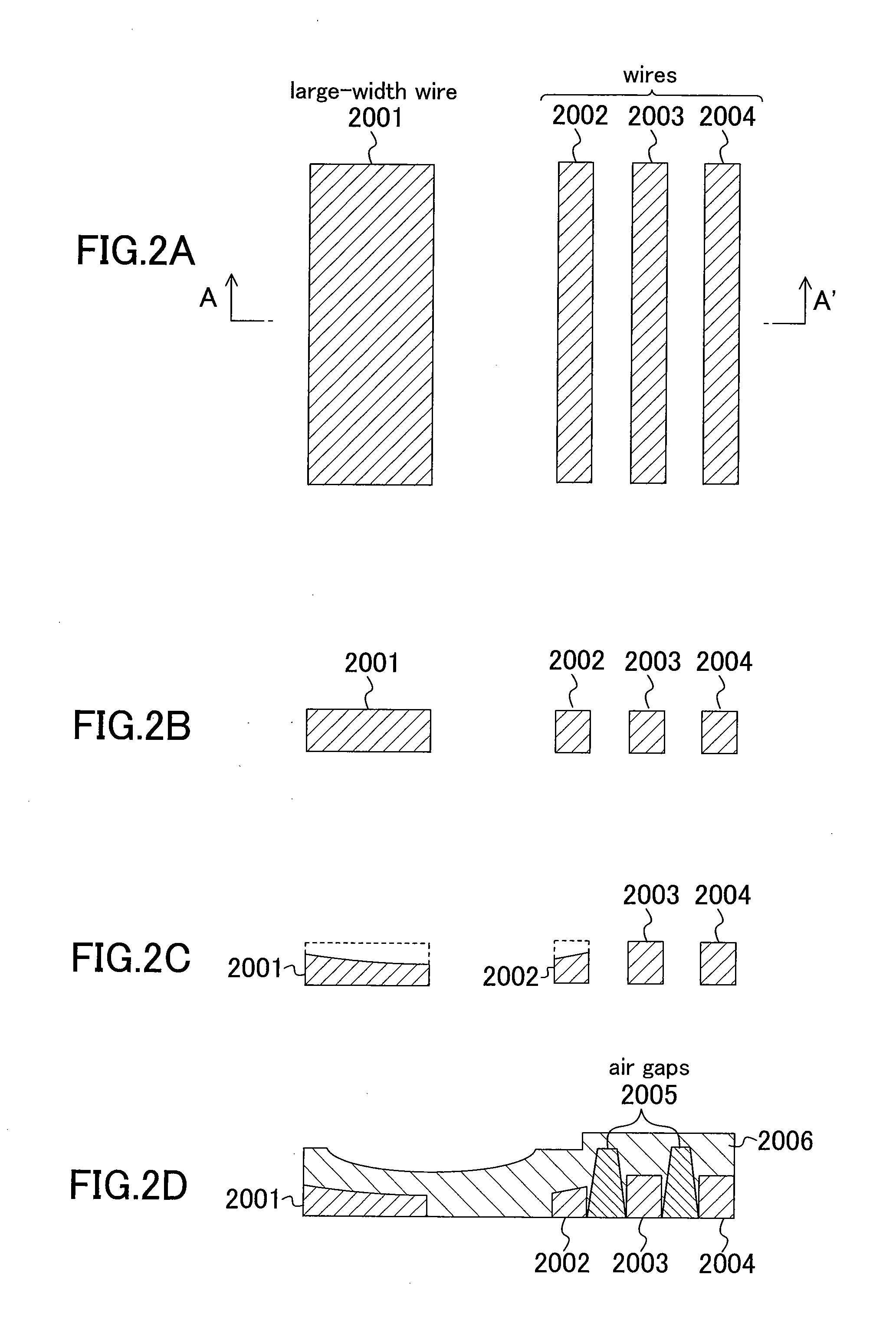
[0097]In this embodiment, by identifying a step appearing portion and forming an air gap-forbidden region with respect to the step appearing portion, a top portion of an air gap is prevented from being removed by CMP.
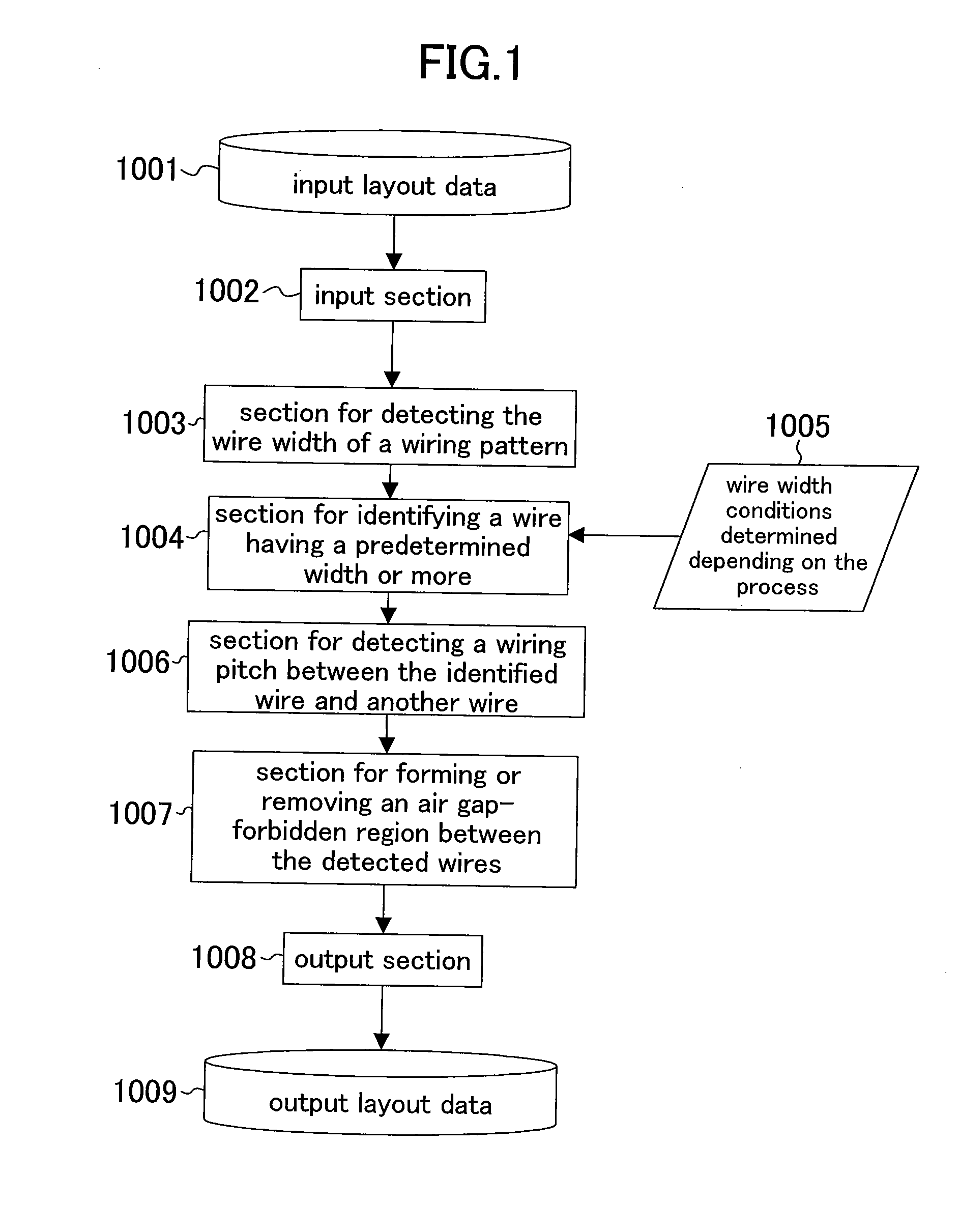
[0098]FIG. 1 is a diagram schematically showing a configuration of the wiring structure designing device of the first embodiment of the present invention.
[0099]In FIG. 1, the wiring structure designing device of the semiconductor integrated circuit device comprises an input section 1002 for inputting data 1001 of a layout after wiring, a section 1003 for detecting a wire width of each wire in a wiring pattern of the input layout data 1001, a section 1004 for identifying a wire having a predetermined width or more based on the result of detection by the secti...
second embodiment
[0126]Hereinafter, a wiring structure designing device according to a second embodiment of the present invention and a wiring structure obtained by the designing device will be described.
[0127]The wiring structure designing method and device of the first embodiment forbid the formation of an air gap in all of large-width wires, high-density wiring regions, and their vicinities, so that a more number of air gaps than necessary are not formed, and therefore, the low-k property may be hindered.
[0128]In this embodiment, by calculating the level of a step of wires, it is determined whether or not an air gap will be formed, instead of forbidding the formation of all air gaps that satisfy conditions which are determined, depending on the process.
[0129]FIG. 8 is a diagram schematically showing a configuration of the wiring structure designing device of the second embodiment of the present invention.
[0130]In FIG. 8, the device for designing a wiring structure of a semiconductor integrated ci...
third embodiment
[0138]Hereinafter, a wiring structure designing method according to a third embodiment of the present invention and a wiring structure obtained by the designing method will be described.
[0139]In this embodiment, an air gap and an air gap-forbidden region are formed between wires under conditions that an air gap-forbidden region is not provided in an entire portion having a predetermined area or more between wires, and an air gap and an air gap-forbidden region are formed in such a portion, so that an air gap can be efficiently formed in portions where an area between wires has a predetermined value or more.
[0140]FIG. 10 is a flowchart showing a process flow of the wiring structure designing method of the third embodiment of the present invention.
[0141]Hereinafter, the process flow of FIG. 10 will be described.
[0142]Initially, in a step (wiring pitch detecting step) S0010_001, a space between wires in which an air gap can be formed (air gap formable region) is detected in a whole chi...
PUM
 Abstract
Description
Claims
Application Information
 - R&D Engineer
- R&D Manager
- IP Professional
- Industry Leading Data Capabilities
- Powerful AI technology
- Patent DNA Extraction
Browse by: Latest US Patents, China's latest patents, Technical Efficacy Thesaurus, Application Domain, Technology Topic.
© 2024 PatSnap. All rights reserved.Legal|Privacy policy|Modern Slavery Act Transparency Statement|Sitemap