
Non-volatile memory device and method of operating the same

a non-volatile memory and non-volatile technology, applied in semiconductor devices, digital storage, instruments, etc., can solve the problems of low reliability of prams and cbrams at high temperatures, and the conductive bridge is destroyed, and achieves low resistance and high resistance

Inactive Publication Date: 2008-07-03
SAMSUNG ELECTRONICS CO LTD
View PDF3 Cites 4 Cited by
  • Summary
  • Abstract
  • Description
  • Claims
  • Application Information

AI Technical Summary

Benefits of technology

[0009]The present invention provides a non-volatile memory device using a change in resistance in a junction portion between a metal electrode and a chalcogenide material layer to realize information storage states without being affected by high temperatures, and a method of operating the non-volatile memory device.
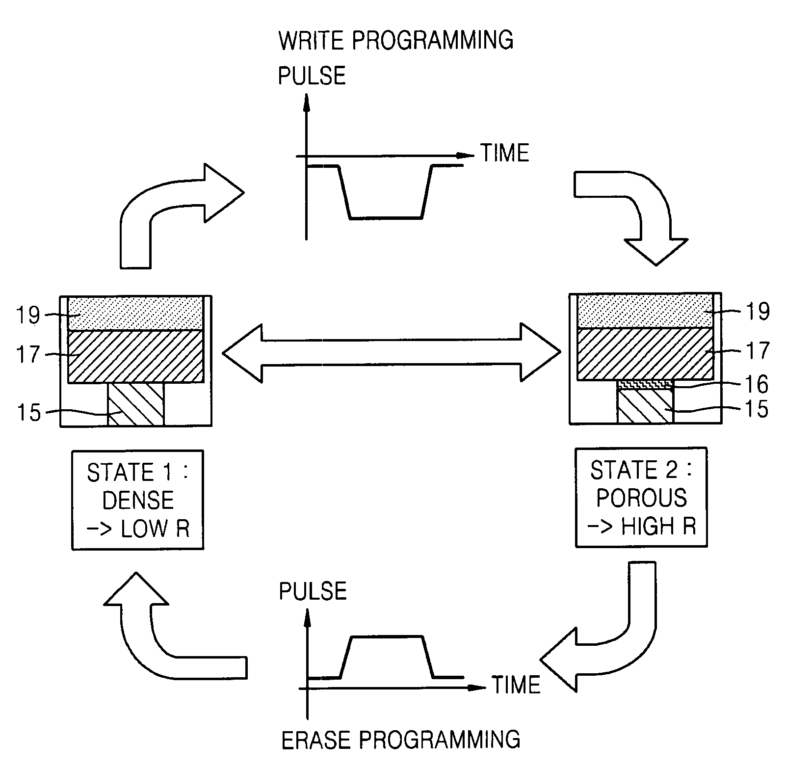
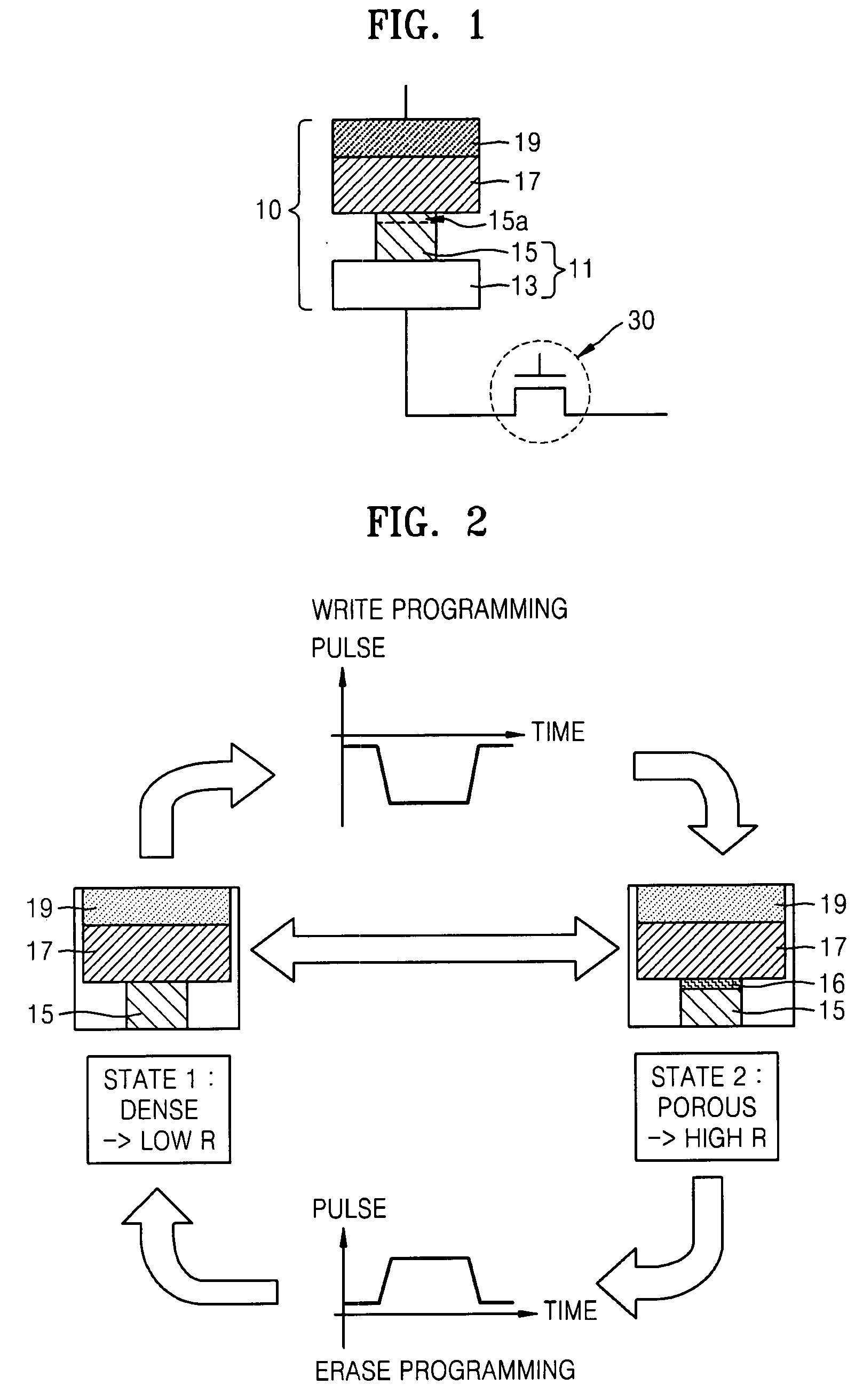
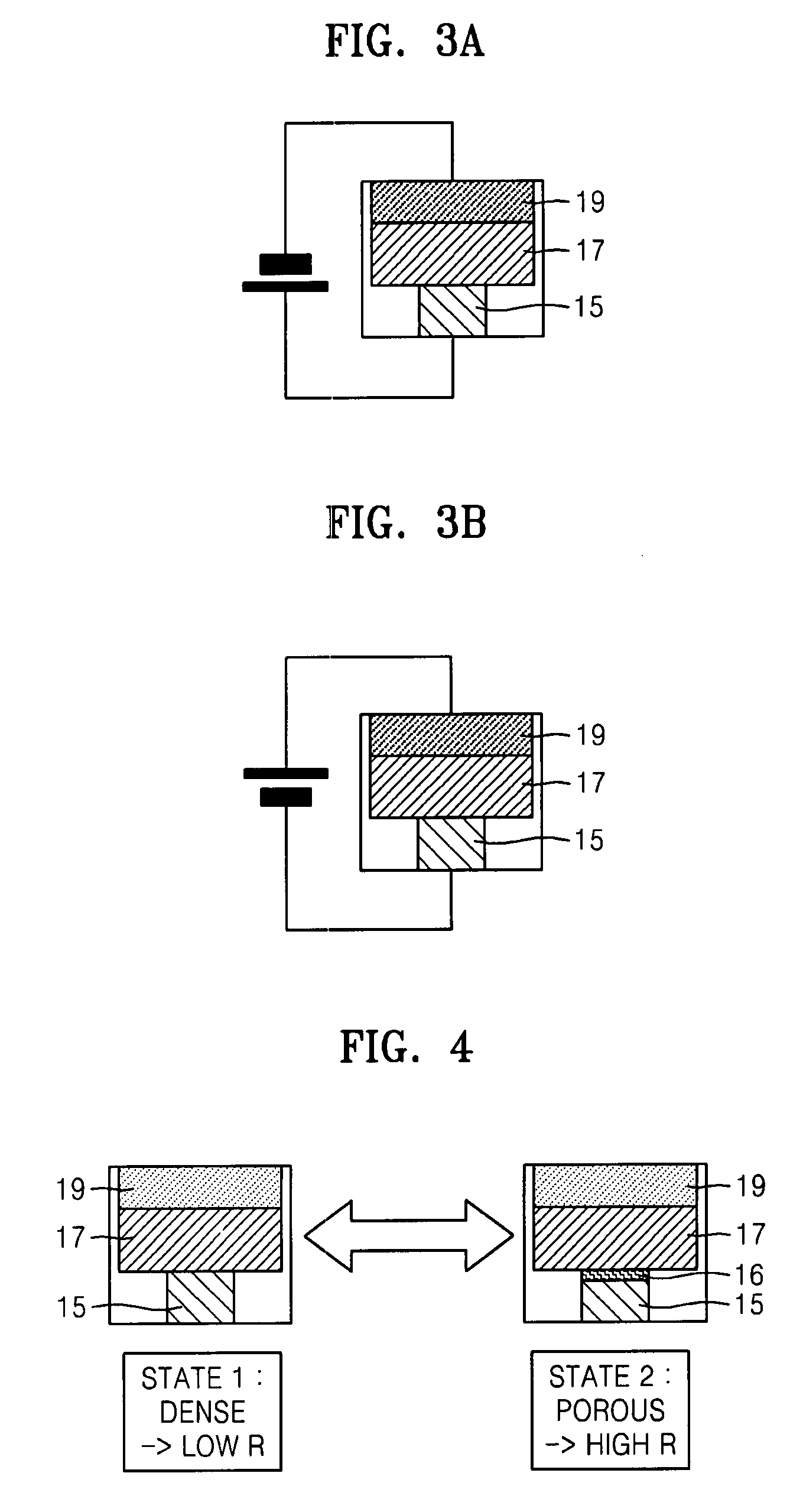
[0018]A region of the electrode contact adjacent to the chalcogenide material layer may become porous when applying a pulse current to the chalcogenide material layer from the electrode contact layer, thereby forming a high resistance state, and the region of the electrode contact layer adjacent to the chalcogenide material layer may become a dense conductive material when applying a pulse current to the electrode contact layer from the chalcogenide material layer, thereby forming a low resistance state.

Problems solved by technology

However, the problem of the PRAM is that the amorphous phase storing information is crystallized at a high temperature, and the problem of the CBRAM is that a conductive bridge is destroyed at a high temperature due to activated movement of atoms.
Thus the PRAM and CBRAM have low reliability at high temperatures.

Method used


Image

  • Non-volatile memory device and method of operating the same
  • Non-volatile memory device and method of operating the same
  • Non-volatile memory device and method of operating the same

Examples


Embodiment Construction

[0031]The present invention will now be described more fully with reference to the accompanying drawings, in which exemplary embodiments of the invention are shown.

[0032]FIG. 1 is a schematic view of a non-volatile memory device according to an embodiment of the present invention.

[0033]Referring to FIG. 1, the non-volatile memory device includes a storage node 10 and a switching device 30 connected to the storage node 10. The switching device 30 is preferably a field effect transistor, but may also be a transistor, a PN diode, or a bipolar junction transistor. The switching device 30 may be one of various switching devices having various structures that are known in the field of memory devices.

[0034]The storage node 10 includes a first electrode 11 connected to the switching device 30, a chalcogenide material layer 17 formed on the first electrode 11, and a second electrode 19 formed on the chalcogenide material layer 17.

[0035]The first electrode 11 includes an electrode contact lay...


PUM


Abstract

Provided are a non-volatile memory device and a method of operating the non-volatile memory device. The non-volatile memory device includes a switching device and a storage node connected to the switching device, wherein the storage node comprises: a first electrode connected to the switching device; a chalcogenide material layer formed on the first electrode; and a second electrode formed on the chalcogenide material layer, and one of the first and second electrodes comprises an electrode contact layer formed adjacent to a limited region of the chalcogenide material layer, and a property of the electrode region adjacent to the chalcogenide material layer is changed reversibly according to the direction in which a current is applied, thereby changing between a high resistance state and a low resistance state.

Description

CROSS-REFERENCE TO RELATED PATENT APPLICATION[0001]This application claims the benefit of Korean Patent Application No. 10-2006-0138860, filed on Dec. 29, 2006 in the Korean Intellectual Property Office, the disclosure of which is incorporated herein in its entirety by reference.BACKGROUND OF THE INVENTION[0002]1. Field of the Invention[0003]The present invention relates to a non-volatile memory device and a method of operating the non-volatile memory device, and more particularly, to a non-volatile memory device using a change in resistance in a junction portion between a metal electrode and a chalcogenide material layer, and a method of operating the non-volatile memory device.[0004]2. Description of the Related Art[0005]Examples of non-volatile memory devices using a change in resistance in a junction portion between a metal electrode and a chalcogenide material layer are a phase change random access memory (PRAM) and a conducting bridge memory (CBRAM).[0006]A CBRAM stores inform...

Claims


Application Information

Patent Timeline
Patent Type & Authority Applications(United States)
IPC IPC(8): G11C11/00H01L45/00H10B69/00
CPCG11C13/0004G11C13/0069G11C13/02G11C2013/0073G11C2213/56G11C2213/79Y10S977/754H01L27/2436H01L45/085H01L45/1233H01L45/1266H01L45/144H01L27/2409H10B63/20H10B63/30H10N70/245H10N70/8416H10N70/826H10N70/8828H10N70/061
Inventor SUH, DONG-SEOKLEE, JUN-HO
Owner SAMSUNG ELECTRONICS CO LTD
Learn More