Level shifter for use between voltage domains

Inactive Publication Date: 2008-07-03
ARM LTD
View PDF5 Cites 8 Cited by
  • Summary
  • Abstract
  • Description
  • Claims
  • Application Information

AI Technical Summary

Benefits of technology

[0015]The present technique recognises that latency can be reduced by using a first and a second buffer circuit, directly coupling the signals from the first buffer circuit to the second buffer circuit and providing a feedback circuit operating away from the critical path to boost the non-common voltage level signal supplied by the first buffer circuit to the voltage level being used by the second buffer circuit in the second domain and thereby properly switch off the relevant transistors within the second buffer circuit so as to reduce the static power consumption thereof. In this way, the level shifter circuit of the present technique is able to combine reduced latency with low static power consumption.
[0016]The level shifter circuit can be provided between different voltage domains which have variable supply voltages, such that sometimes the supply voltages are the same and sometimes they are different. The level shifter circuit provides reduced latency without a dependence upon whether there is a voltage difference.
[0018]The circuit within the first domain which drives the feedback signal to the first voltage level can be provided in a number different ways, but is advantageously provided in the form of a feedback signal initiating transistor receiving the input signal in parallel with the first buffer circuit. Placing the feedback signal initiating transistor in parallel with the first buffer circuit means that generation of the feedback signal is rapid with no additional latency consequent to the signal having first to propagate through the first buffer circuit.
[0019]Further speed gains may be achieved by the provision of a feedback signal boost transistor operating in the second voltage domain and coupled to the feedback signal initiating circuit and responsive to the intermediate signal to boost the feedback signal to the second voltage level in cooperation with the feedback circuit. This raises the rise time of the feedback circuit and speeds switching.
[0020]Whilst the provision of the feedback circuit to boost the feedback signal to the full voltage level in the second domain is advantageous in reducing static power consumption, the action of the feedback circuit will tend to resist changes in the level of the feedback signal, and thereby slow switching operation. In order to help reduce this phenomenon, the feedback circuit is coupled to the second voltage supplied by one or more supply interrupting transistors controlled by the input signal to temporarily interrupt feedback operation of the feedback circuit and thereby reduce the action of the feedback circuit in registering changes in the feedback signal.
[0023]Whilst the present technique can be used in a wide variety of applications, it is particularly useful when the level shifter circuit is part of an integrated circuit and when the second voltage domain includes a memory circuit operating with the second voltage supply so as to enhance data retention within that memory circuit.

Problems solved by technology

Typically, such multiple domain arrangements were not used in high performance systems due to the increased complexity and the relatively long latency which is associated with level shifter circuits.
With the reduction in size of process geometries, such SRAM cells are becoming less stable.
A problem with this simple arrangement is that the desirable situation of a low static power consumption is difficult to achieve within the second inverter 4 since the signal from the first inverter 2 at the VDD level of the first domain is ineffective at completely switching off the transistors within the second inverter 4 given its higher VDD level.
In addition, the current during switching of the second inverter 4 is undesirably high.
However, the circuit of FIG. 2 suffers from a limited range of voltage level shifting within which it may operate since the input inverter 10 may not be strong enough to overcome the action of the feedback PMOS 6 if the low voltage domain is operating at a significantly lower VDD level than the high voltage domain.
A significant disadvantage of the circuit of FIG. 3 is that it has a disadvantageously long latency since it is necessary when the input is changed to a “0” for this change to propagate through four levels of transistors, namely through inverter 24, NMOS transistor 26, PMOS transistor 12 and inverter 22.

Method used


Image

  • Level shifter for use between voltage domains
  • Level shifter for use between voltage domains
  • Level shifter for use between voltage domains

Examples


Embodiment Construction

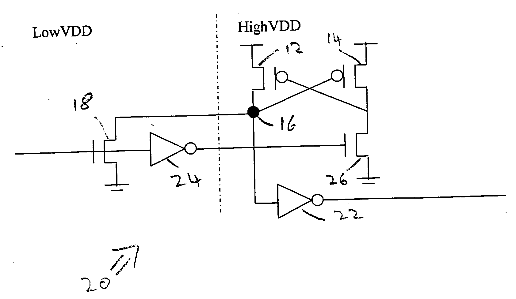
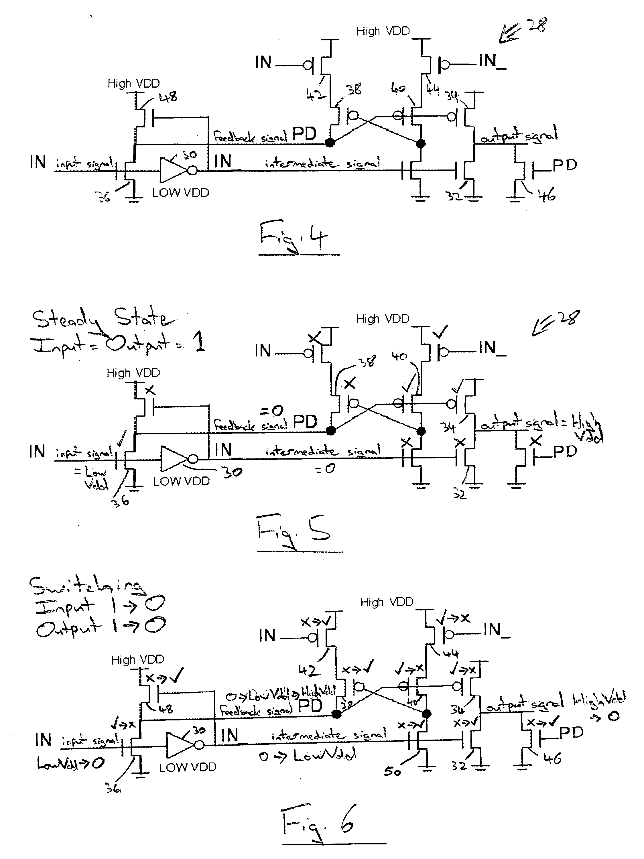
[0049]FIG. 4 shows a level shifter circuit 28 comprising a first buffer circuit in the form of an inverter 30 and a second buffer circuit in the form of a transistor stack comprising transistors 32 and 34. An input signal is applied in parallel to the inputs of an NMOS transistor 36 and the inverter 30. The NMOS transistor 36 serves as a feedback signal initiating transistor. Cross-coupled PMOS transistors 38 and 40 serve as a feedback circuit. Supply interrupting transistors 42 and 44 serve to temporarily interrupt the power supply to the cross-coupled PMOS transistors 38 and 40 in response to the input signal and the inverted input signal respectively, and output boost transistor 46, comprising an NMOS transistor switched by the feedback signal, is coupled to the NMOS transistor 32 of the second buffer circuit and serves to increase the speed at which the output signal falls to a “0” (ground / common voltage level) when the input signal is changed from a “1” to a “0”.

[0050]Within th...


PUM


Abstract

A level shifter circuit 28 has a first buffer circuit 30 and a second buffer circuit 32, 34. An intermediate signal generated by the first buffer circuit 30 is directly passed to the second buffer circuit 32, 34 to control output of one of its output signal levels. A feedback signal generated in response to the input signal within the first power domain containing the first buffer circuit 30 is passed directly to the second buffer circuit 32, 34 to control the output signal level reaching the other of the output values. A feedback circuit comprising cross-coupled PMOS transistors 38, 40 is provided to boost the feedback signal level up to the voltage level of the second voltage domain which contains the feedback circuit 38, 40 as well as the second buffer circuit 32, 34. The level shifter circuit 28 has a low latency and a low static power consumption.

Description

BACKGROUND OF THE INVENTION[0001]1. Field of the Invention[0002]This invention relates to the field of level shifter circuits for use between voltage domains, such as, for example, different voltage domains within an integrated circuit.[0003]2. Description of the Prior Art[0004]A level shifter circuit is used when there is a need to pass signals from one voltage domain to a different voltage domain. Typically, such multiple domain arrangements were not used in high performance systems due to the increased complexity and the relatively long latency which is associated with level shifter circuits.[0005]A trend within integrated circuits is the increasingly common use of embedded SRAM memory. With the reduction in size of process geometries, such SRAM cells are becoming less stable. In order to enhance the stability of SRAM provided on-chip, and still achieve low power for the processor, there is an increasing need for the SRAM and the processor to use different voltage supplies from d...

Claims


Application Information

Patent Timeline
IPC IPC(8): H03L5/00
CPCH03K3/356113H03K19/018528H03K19/01714
Inventor YEUNG, GUS
Owner ARM LTD
Why Eureka
Try Eureka