Eureka AIR delivers breakthrough ideas for toughest innovation challenges, trusted by R&D personnel around the world.

Controlled buckling structures in semiconductor interconnects and nanomembranes for stretchable electronics

a technology of nanomembranes and semiconductors, applied in the direction of thermoelectric devices, semiconductor/solid-state device details, dielectric characteristics, etc., can solve the problems of inability to bind to inorganic semiconductors, and inability to bind to most flexible materials. , to achieve the effect of precise and accurate geometric construction, flexible and bendability, and without adversely affecting performan

Active Publication Date: 2008-07-03
THE BOARD OF TRUSTEES OF THE UNIV OF ILLINOIS
View PDF98 Cites 384 Cited by
  • Summary
  • Abstract
  • Description
  • Claims
  • Application Information

AI Technical Summary

Benefits of technology

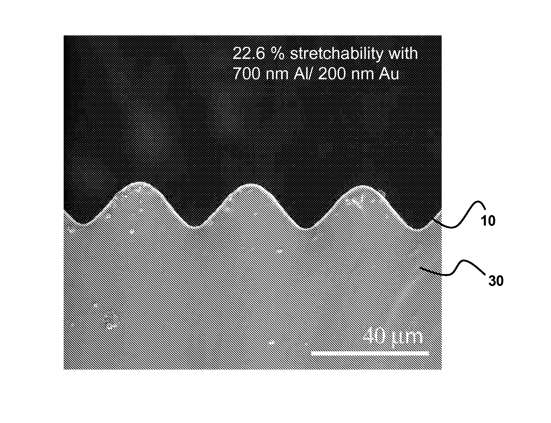
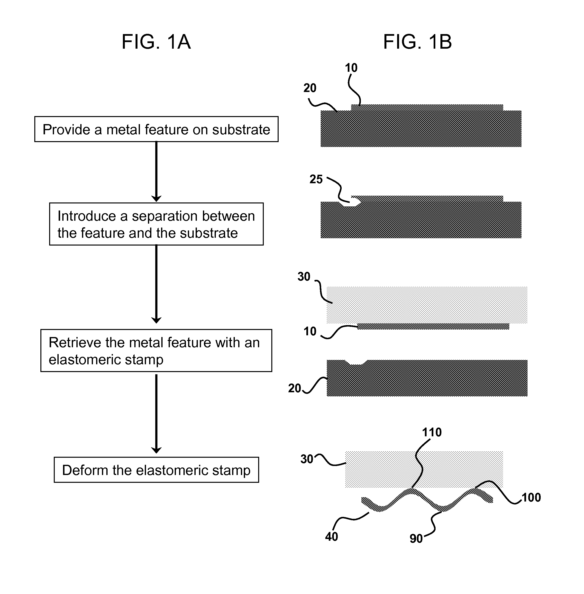
[0012]The present invention provides stretchable devices and device components such as semiconductors and stretchable electronic devices, and circuits. Stretchable, bendable and conformable electronic devices and device components are required for making electronics suitable for printing on a variety of curved surfaces. Shape-conforming devices have a variety of applications ranging from flexible displays and electronic fabrics to conformable biological and physical sensors. Accordingly, an embodiment of the invention are flexible and bendable electronic devices, device components, and related methods for making flexible and bendable devices. Such flexibility and bendability is accomplished by providing an interconnect or semiconductor membrane having a wavy or buckled geometry. Such geometry provides a means for ensuring the system is stretchable and bendable without adversely impacting performance, even under vigorous and repeated stretching and / or bending cycles. Furthermore, the methods provide a capability of precise and accurate geometric construction, so that physical characteristics (e.g., stretchability, bendability) of the device and / or device component may be tailored to the operating conditions of the system. Another aspect of the invention are stretchable components having a physical property that is at least partially coupled to strain, so that the parameter is capable is capable of being tuned by application of varying amount of strain to the component.
[0013]An array of device components may be connected to one another by buckled components or interconnects, to facilitate independent movement of device components relative to one another. Local regions within the array, however, may have a different bending or stretching requirement than other regions. The devices and methods presented herein facilitate construction of a flexible system that can have localized variation in buckled component or interconnect geometry including component or interconnect dimension, periodicity, amplitude, orientation, and total number of components or interconnects in an area, for example. Generating multiple components or interconnects having controllable orientation facilitates tailoring components or interconnects to the device's operating conditions.
[0028]In an embodiment, a device array has sets of components that are oriented in at least two different directions. For example, in a grid configuration the components may have two orientations that are perpendicular or orthogonal to one another to provide capacity for stretching in two directions. In another embodiment, the device array may comprise components that are all aligned with respect to each other. That embodiment may be useful where stretching or bending is confined to a single direction (e.g., bending an electronic device fabric to a cylindrical surface). Additional bending and / or stretching capacity is provided by orienting the components in three or more directions, three directions or four directions, for example. In an embodiment, additional control and stability is provided by having the components of the device array placed in any number of different layers, such as two layers adjacent to one another.
[0037]In another embodiment, any of the methods or devices have an elastomeric substrate with a plurality of compliant regions and a plurality of rigid regions. Such a substrate provides flexural rigidity of the compliant regions that is less than that of the rigid regions, and optionally have the first and second ends of each of the stretchable components bonded to at least one of the rigid regions and a central region of each of the stretchable components bonded to at least one of the compliant regions. Use of this substrate type provides the capacity of achieving controllable buckling of the component based on the pattern of compliancy of the underlying substrate.
[0048]In an embodiment, the invention relates to methods and structures having a wavy nanomembrane, such as a wavy semiconductor nanomembrane. Such a wavy nanomembrane facilitates incorporation of flexibility in a device component itself (in contrast to flexibility of the interconnects that connect device components). In an aspect, the invention is a method of making a biaxially stretchable semiconductor membrane transferring a semiconductor nanomembrane material from a first substrate to a second deformed substrate, wherein after transfer the deformed substrate is permitted to relax back to its resting configuration. In an aspect, the thickness of the semiconductor material is between about 40 nm and 600 nm. Release of a two-dimensional deforming force generates a nanomembrane having a two-dimensional wavy structure. In an aspect, the deforming force is generated by changing the temperature of the flexible substrate.
[0053]Useful contact printing methods for assembling, organizing and / or integrating printable semiconductor elements in the present methods include dry transfer contact printing, microcontact or nanocontact printing, microtransfer or nanotransfer printing and self assembly assisted printing. Use of contact printing is beneficial in the present invention because it allows assembly and integration of a plurality of printable semiconductor in selected orientations and positions relative to each other. Contact printing in the present invention also enables effective transfer, assembly and integration of diverse classes of materials and structures, including semiconductors (e.g., inorganic semiconductors, single crystalline semiconductors, organic semiconductors, carbon nanomaterials etc.), dielectrics, and conductors. Contact printing methods of the present invention optionally provide high precision registered transfer and assembly of printable semiconductor elements in preselected positions and spatial orientations relative to one or more device components prepatterned on a device substrate. Contact printing is also compatible with a wide range of substrate types, including conventional rigid or semi-rigid substrates such as glasses, ceramics and metals, and substrates having physical and mechanical properties attractive for specific applications, such as flexible substrates, bendable substrates, shapeable substrates, conformable substrates and / or stretchable substrates. Contact printing assembly of printable semiconductor structures is compatible, for example, with low temperature processing (e.g., less than or equal to 298K). This attribute allows the present optical systems to be implemented using a range of substrate materials including those that decompose or degrade at high temperatures, such as polymer and plastic substrates. Contact printing transfer, assembly and integration of device elements is also beneficial because it can be implemented via low cost and high-throughput printing techniques and systems, such as roll-to-roll printing and flexographic printing methods and systems.

Problems solved by technology

The design and fabrication of flexible electronic devices exhibiting good electronic performance, however, present a number of significant challenges.
First, the well developed methods of making conventional silicon based electronic devices are incompatible with most flexible materials.
In addition, most inorganic semiconductors are not intrinsically soluble in convenient solvents that would allow for solution based processing and delivery.
Second, although many amorphous silicon, organic or hybrid organic-inorganic semiconductors are compatible with incorporation into flexible substrates and can be processed at relatively low temperatures, these materials do not have electronic properties capable of providing integrated electronic devices capable of good electronic performance.
As a result of these limitations, flexible electronic devices are presently limited to specific applications not requiring high performance, such as use in switching elements for active matrix flat panel displays with non-emissive pixels and in light emitting diodes.
These circuits often are unable to sufficiently conform to their surroundings because of an inability of the conducting components to stretch in response to conformation changes.
Accordingly, those flexible circuits are prone to damage, electronic degradation and can be unreliable under rigorous and / or repeated conformation change.
The drawbacks of a conductive rubber include high electrical resistivity and significant resistance changes under stretching, thereby resulting in overall poor interconnect performance and reliability.
That system suffers limitations in the ability to controllably and precisely pattern in different shapes and in additional planes, thereby limiting the ability to tailor systems to different strain and bending regimes.
Those metal cracks, however, are not compatible with thick metal films, and instead is compatible with a rather narrow range of thin metal films (e.g., on the order of less than 30 nm) that are deposited on top of patterned elastomer.
That study, however, used comparatively thin layers of metal films (e.g., about 105 nm) and is relatively limited in that the system could potentially make electrical conductors that could be stretched by about 10%.

Method used


Image

  • Controlled buckling structures in semiconductor interconnects and nanomembranes for stretchable electronics
  • Controlled buckling structures in semiconductor interconnects and nanomembranes for stretchable electronics
  • Controlled buckling structures in semiconductor interconnects and nanomembranes for stretchable electronics

Examples


example 1

Controlled Buckling Structures in Semiconductor Nanoribbons With Application Examples in Stretchable Electronics

[0180]Control over the compositions, shapes, spatial locations and / or geometrical configurations of semiconductor nanostructures is important for nearly all applications of these materials. Although methods exist for defining the material compositions, diameters, lengths, and positions of nanowires and nanoribbons, there are relatively few approaches for controlling their two- and three-dimensional (2D and 3D) configurations. Provided herein is a mechanical strategy for creating certain classes of 3D shapes in nanoribbons that are otherwise difficult to generate. This example involves the combined use of lithographically patterned surface chemistry to provide spatial control over adhesion sites and elastic deformations of a supporting substrate to induce well-controlled local displacements. Precisely engineered buckling geometries are created in nanoribbons of GaAs and Si ...

example 2

Transfer Printing

[0202]Our technical approach uses certain ideas embodied in the planar stamp based printing methods previously described. Although these basic techniques provide a promising starting point, many fundamentally new features must be introduced to meet the challenges of the HARDI (Hemispherical Array Detector for Imaging) system, as described in the following.

[0203]FIGS. 32 and 33 illustrate a general strategy related to transfer printing to curved surfaces. The first set of steps (FIG. 32) involves the fabrication and manipulation of a thin, spherically curved elastomeric stamp designed to lift off interconnected Si CMOS ‘chiplets’ from the planar surface of a wafer and then to transform the geometry into a hemispherical shape. A stamp for this process is formed by casting and curing a liquid prepolymer to obtain an elastomer such as poly(dimethylsiloxane) (PMDS) against high quality optical elements (i.e. a matched pair of convex and concave lenses) selected with the ...

example 3

Biaxially Stretchable “Wavy” Silicon Nanomembranes

[0214]This example introduces a biaxially stretchable form of single crystalline silicon that consists of two dimensionally buckled, or “wavy”, silicon nanomembranes on elastomeric supports. Fabrication procedures for these structures are described, and various aspects of their geometries and responses to uniaxial and biaxial strains along various directions are presented. Analytical models of the mechanics of these systems provide a framework for quantitatively understanding their behavior. These classes of materials provides a route to high-performance electronics with full, two-dimensional stretchability.

[0215]Electronics that offer mechanically bendability are of interest for applications in information display, X-ray imaging, photovoltaic devices, and other systems. Reversible stretchability is a different and much more technically challenging mechanical characteristic that would enable device possibilities that cannot be realiz...


PUM

PropertyMeasurementUnit
Fractionaaaaaaaaaa
Fractionaaaaaaaaaa
Fractionaaaaaaaaaa

Abstract

In an aspect, the present invention provides stretchable, and optionally printable, components such as semiconductors and electronic circuits capable of providing good performance when stretched, compressed, flexed or otherwise deformed, and related methods of making or tuning such stretchable components. Stretchable semiconductors and electronic circuits preferred for some applications are flexible, in addition to being stretchable, and thus are capable of significant elongation, flexing, bending or other deformation along one or more axes. Further, stretchable semiconductors and electronic circuits of the present invention are adapted to a wide range of device configurations to provide fully flexible electronic and optoelectronic devices.

Description

CROSS-REFERENCE TO RELATED APPLICATIONS[0001]This application claims the benefit of U.S. Provisional Patent Applications 60 / 944,626 filed Jun. 18, 2007 and 60 / 824,683 filed Sep. 6, 2006 and is a continuation-in-part of U.S. patent application Ser. Nos. 11 / 145,574 filed Jun. 2, 2005, and 11 / 145,542 filed Jun. 2, 2005, each of which claim benefit of U.S. Provisional Patent Application Nos. 60 / 577,077, 60 / 601,061, 60 / 650,305, 60 / 663,391 and 60 / 677,617 filed on Jun. 4, 2004, Aug. 11, 2004, Feb. 4, 2005, Mar. 18, 2005, and May 4, 2005, respectively, and is also a continuation-in-part of Ser. No. 11 / 423,287 filed Jun. 9, 2006 which claims benefit of 60 / 790,104 filed Apr. 7, 2006, and is a continuation-in-part of U.S. patent application Ser. Nos. 11 / 145,574 filed Jun. 2, 2005, and 11 / 145,542 filed Jun. 2, 2005, all of which are hereby incorporated by reference in their entirety to the extent not inconsistent with the disclosure hereinSTATEMENT REGARDING FEDERALLY SPONSORED RESEARCH OR DEVE...

Claims


Application Information

Patent Timeline
IPC IPC(8): H01L29/84H01L21/00H05K1/00
CPCH01L21/02628H05K2201/09045H01L27/12H01L2924/12041H01L21/8258H01L21/02422H05K2203/0271H05K2201/0133H05K3/20H01L2924/13091H05K1/0283H01L29/0657H01L2924/00Y10T29/4913H01L29/72H01L21/4846H01L23/5387H05K3/22
Inventor ROGERS, JOHN A.MEITL, MATTHEWSUN, YUGANGKO, HEUNG CHOCARLSON, ANDREWCHOI, WON MOOKSTOYKOVICH, MARKJIANG, HANQINGHUANG, YONGGANG
Owner THE BOARD OF TRUSTEES OF THE UNIV OF ILLINOIS
Why Eureka
Eureka Blog
Learn More