Pwm drive apparatus and method for correcting output offset thereof
- Summary
- Abstract
- Description
- Claims
- Application Information
AI Technical Summary
Benefits of technology
Problems solved by technology
Method used
Image
Examples
first embodiment
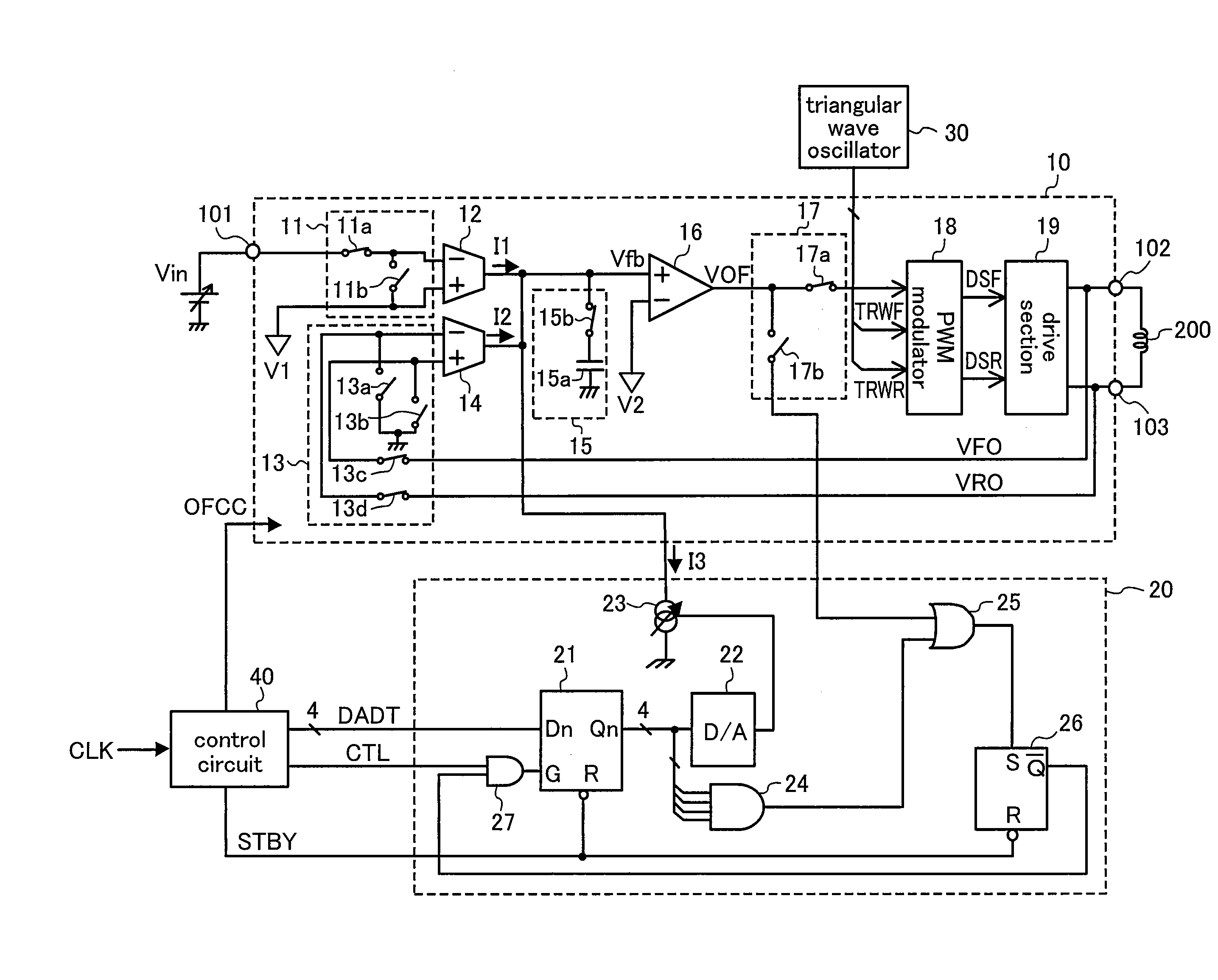
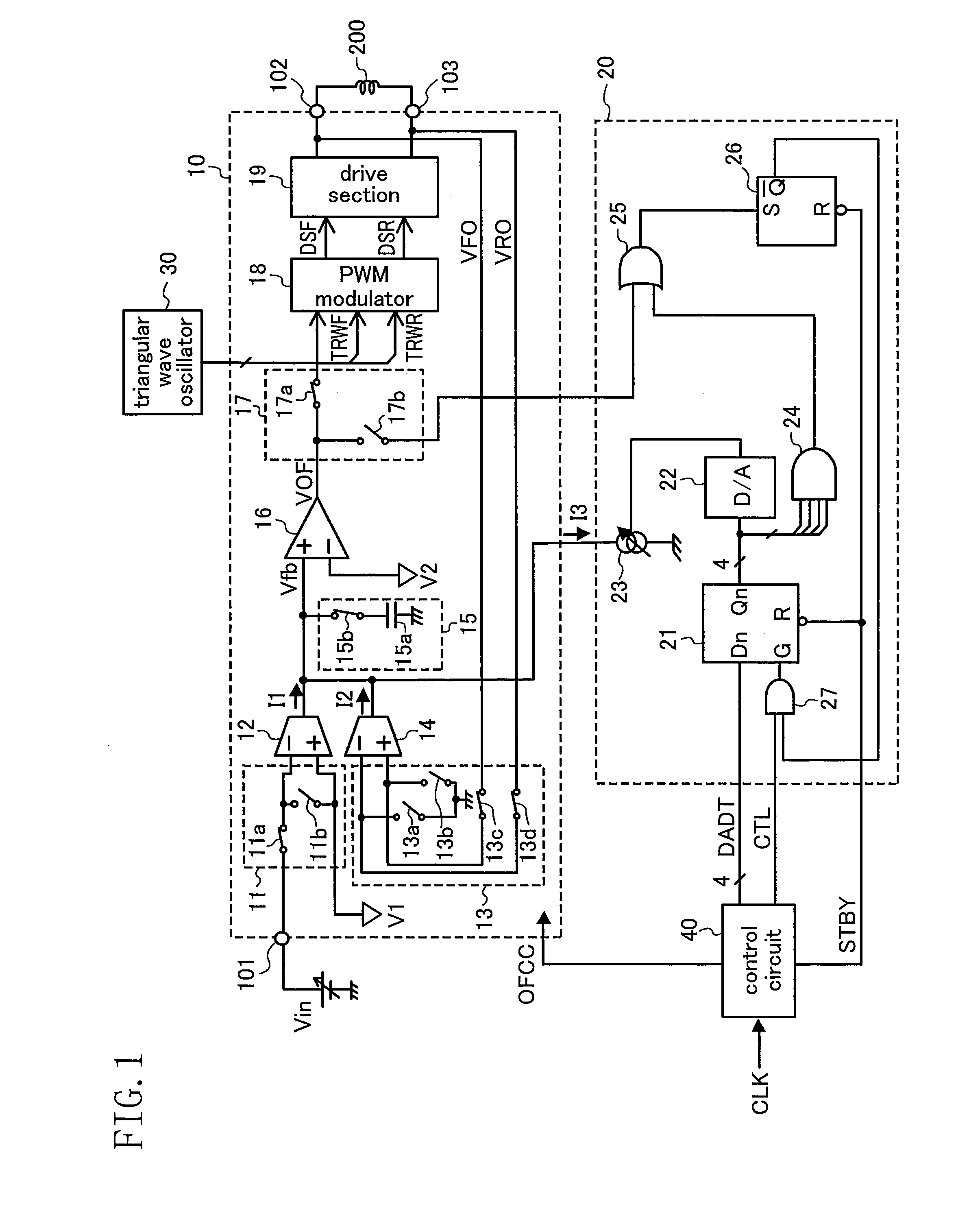
[0037]FIG. 1 shows a structure of a PWM drive apparatus according to a first embodiment. The PWM drive apparatus comprises a PWM driver 10, an offset correcting circuit 20, a triangular wave oscillator 30, and a control circuit 40.
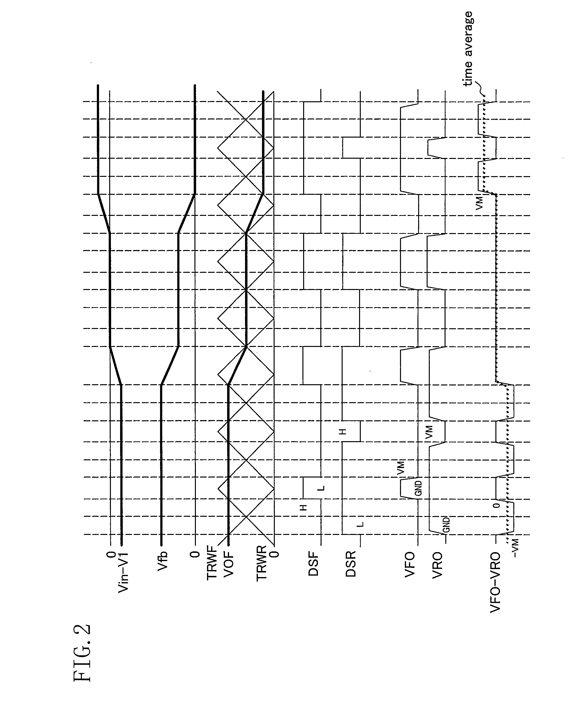
[0038]Firstly, a detailed structure of the PWM driver 10 will be described. A command voltage Vin applied to an input terminal 101 and a reference voltage V1 are input via a switch circuit 11 to a negative input terminal and a positive input terminal of a differential-input voltage-to-current converter 12, respectively. The voltage-to-current converter 12 converts a difference voltage between the positive and negative input terminals into a current I1. Voltages VFO and VRO of positive and negative output terminals 102 and 103 are input via a switch circuit 13 to a positive input terminal and a negative input terminal of a differential-input voltage-to-current converter 14, respectively. The voltage-to-current converter 14 converts a difference voltage betw...
second embodiment
[0058]FIG. 6 shows a structure of a PWM drive apparatus according to a second embodiment. This PWM drive apparatus is obtained by adding a delay circuit 28 to the offset correcting circuit 20 of FIG. 1. The delay circuit 28 is provided between the control circuit 40 and the AND gate 27 so as to delay the signal CTL output from the control circuit 40.
[0059]FIG. 7 is a timing chart of the PWM drive apparatus. A difference from the PWM drive apparatus of FIG. 1 is that the signal CTL matches the clock signal CLK. Specifically, the signal CTL is obtained by performing a gate control with respect to the clock signal CLK. The structure of a portion for generating the signal CTL of the control circuit 40 can be further simplified than in the first embodiment in which the signal CTL is obtained by ½-frequency dividing the clock signal CLK. In this embodiment, the signal CTL and the signal DADT have the same edge timing. Nevertheless, by delaying the signal CTL using the delay circuit 28, th...
third embodiment
[0060]FIG. 8 shows a structure of a PWM drive apparatus according to a third embodiment. This PWM drive apparatus is obtained by adding a capacitor 29 to the offset correcting circuit 20 of FIG. 1. The capacitor 29 is connected to the connection point of the output terminals of the voltage-to-current converters 12 and 14.
[0061]The operation timing of the PWM drive apparatus is the same as that of FIG. 7. Specifically, the signal CTL is obtained by performing a gate control with respect to the clock signal CLK. Therefore, although a noise current occurs in the variable current source 23 due to glitch noise which occurs during a latch operation by the latch circuit 21, the noise current is absorbed by the capacitor 29. Therefore, the output of the amplifier 16 is not incorrectly inverted, so that the PWM drive apparatus can be normally operated in the correction mode.
PUM
 Abstract
Description
Claims
Application Information
 - R&D
- Intellectual Property
- Life Sciences
- Materials
- Tech Scout
- Unparalleled Data Quality
- Higher Quality Content
- 60% Fewer Hallucinations
Browse by: Latest US Patents, China's latest patents, Technical Efficacy Thesaurus, Application Domain, Technology Topic, Popular Technical Reports.
© 2025 PatSnap. All rights reserved.Legal|Privacy policy|Modern Slavery Act Transparency Statement|Sitemap|About US| Contact US: help@patsnap.com


