Dynamic semiconductor storage device and method for operating same

a semiconductor storage device and random access memory technology, applied in static storage, information storage, digital storage, etc., can solve the problems of amp precharging consumption, drams are remarkably slower in respect of read/write access, amp precharging consumes additional clock cycles, etc., and achieves the effect of increasing the operation speed of an integrated sense amplifier

Inactive Publication Date: 2008-05-22
IBM CORP
View PDF3 Cites 17 Cited by
  • Summary
  • Abstract
  • Description
  • Claims
  • Application Information

AI Technical Summary

Benefits of technology

[0010]An object of the present invention is to provide a dynamic semiconductor storage device and a me...

Problems solved by technology

However, compared with SRAMs, DRAMs are remarkably slower in respect to read/write access.
Consequently, the use of DRAMs is performance limited.
Unfortunately sense amp precharging consumes additional clock cycles because bit lines BL and /BL are precharged to the half power voltage VDD/2.
The additional latency associated with detection and amplification presents another operational difficulty...

Method used


Image

  • Dynamic semiconductor storage device and method for operating same
  • Dynamic semiconductor storage device and method for operating same
  • Dynamic semiconductor storage device and method for operating same

Examples


Embodiment Construction

[0027]Preferred embodiments of the present invention will now be described in detail with reference to the drawings. The same reference numerals are provided for identical or corresponding sections in the drawings, and the same explanation will be quoted for the identical sections.

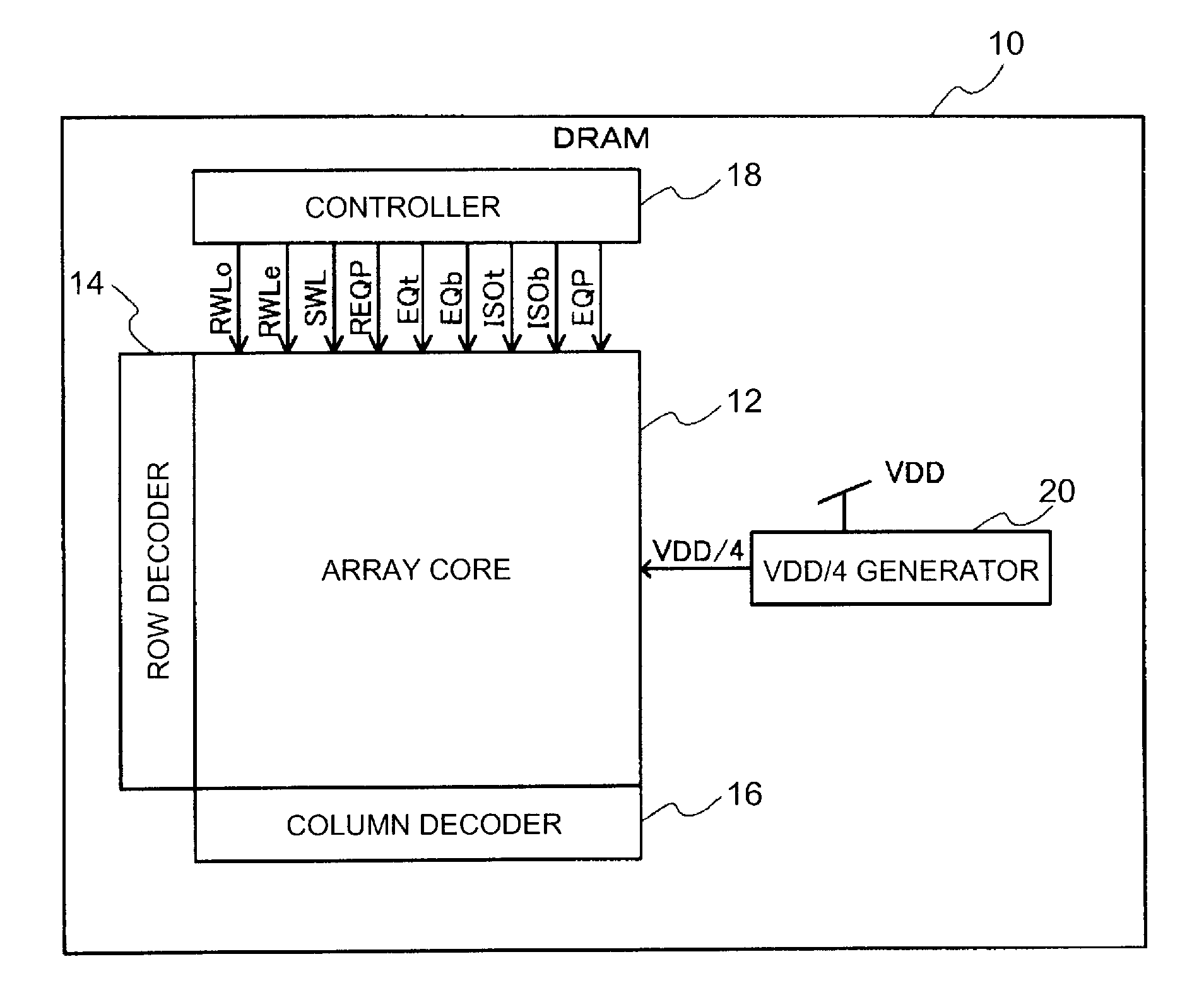
[0028]As shown in FIG. 1, a DRAM 10 according to this embodiment comprises an array core 12, a row decoder 14, a column decoder 16, a controller 18 and a VDD / 4 generator 20. The row decoder 14 selects and drives word lines (not shown) in the array core 12 in response to a row address signal. The column decoder 16 selects and drives column selection lines (not shown) in the array core 12 in response to a column address signal. The controller 18 generates various types of control signals, and transmits them to the array core 12. The VDD / 4 generator 20 generates a quarter power voltage VDD / 4 that is a quarter of a power voltage VDD, and transmits this voltage to the array core 12.

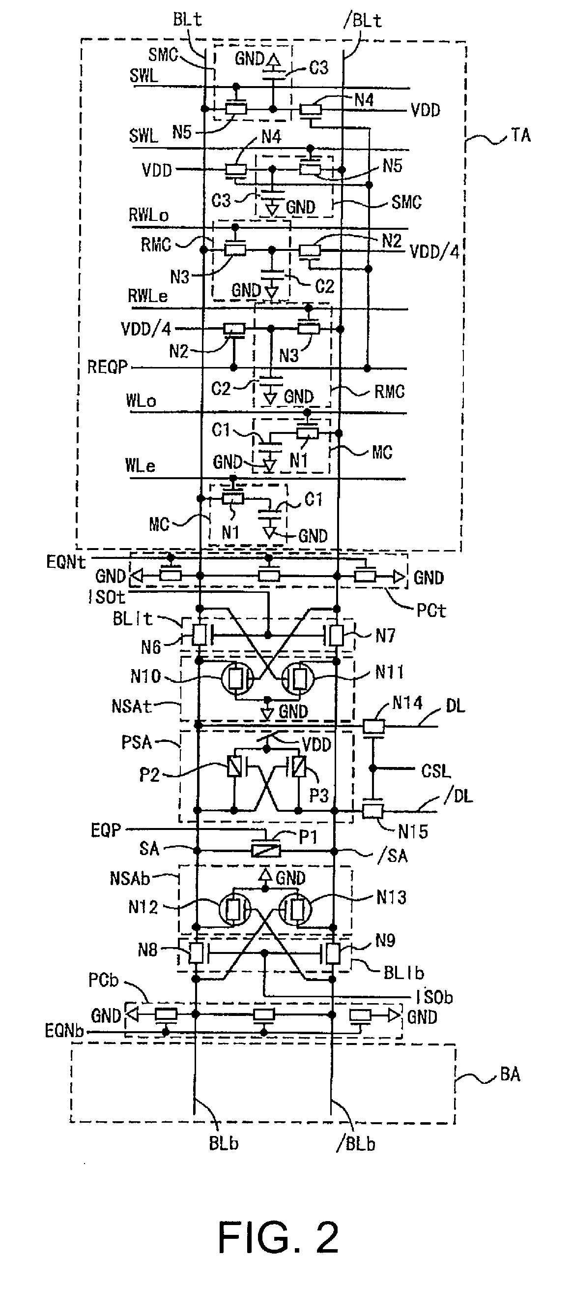
[0029]As shown in FIG. 2, the...


PUM


Abstract

The object of the present invention is to provide a DRAM, in which the operation speed for a sense amplifier can be increased. Bit line precharging circuits PCt and PCb are arranged to precharge bit lines BLt and /BLt to a ground voltage GND, and reference word lines RWLo and RWLe and reference memory cells RMC are arranged, so that when a word line WL is activated, a potential difference is always generated between the bit lines BLt and /BLt. The sources of transistors N10 and N11 of an N-type sense amplifier NSAt are connected directly to a ground terminal GND, and the sources of transistors P2 and P3 of a P-type sense amplifier PSA are connected directly to a power source VDD. The gates of the transistors N10 and N11 are connected to the bit lines /BLt and BLt, and the drains are connected to the bit lines BLt and /BLt, respectively. Shift word lines SWL and shift memory cells SMC are arranged, so that the N sense amplifier NSAt can amplify the potential difference between the bit lines BLt and /BLt.

Description

FIELD OF THE INVENTION[0001]The present invention relates to dynamic random access memory (DRAM) semiconductor storage device and a method for operating the same.BACKGROUND OF THE INVENTION[0002]In various systems applications, SRAMs (Static Random Access Memories), which operate faster than DRAMs, have been employed as routers, hubs or cache memories for CPUs (Central Processing Units). However, the development of highly efficient and multifunctional information and communication systems, mandate an increase in memory capacity. The lower cost per bit of DRAM leads to a more cost efficient storage solution than SRAM. By implementing system storage with DRAM, overall bandwidth can be improved for a wide I / O (input / output) data path or a multibank memory. However, compared with SRAMs, DRAMs are remarkably slower in respect to read / write access. Consequently, the use of DRAMs is performance limited.[0003]Japanese Unexamined Patent Publication (Kokai) No. 2001-84767 (patent document 1) ...

Claims


Application Information

Patent Timeline
IPC IPC(8): G11C7/00
CPCG11C11/4099G11C11/4094
Inventor NAKAMURA, YUTAKA
Owner IBM CORP
Why Eureka
Try Eureka