
Image sensor using thin-film SOI

a thin-film, image sensor technology, applied in the field of image sensors, can solve the problems of kerf loss, disadvantages of poly-crystalline silicon for image sensors, high cost and supply of high-grade silicon and its utilization, etc., to achieve the effect of reducing the need for polishing or furnace annealing of image sensors, improving manufacturing yield, and fast throughpu

Inactive Publication Date: 2008-03-20
CORNING INC
View PDF23 Cites 234 Cited by
  • Summary
  • Abstract
  • Description
  • Claims
  • Application Information

AI Technical Summary

Benefits of technology

[0029]The advantages of this invention are best understood after reading the detailed technical description, and in relation to existing SOI processes. Nonetheless, the primary advantages include: image sensor structure variation; thinner silicon films; more uniform silicon films with higher crystal quality; faster manufacturing throughput; improved manufacturing yield; reduced contamination; and scalability to large substrates. These benefits naturally combine to reduce costs.
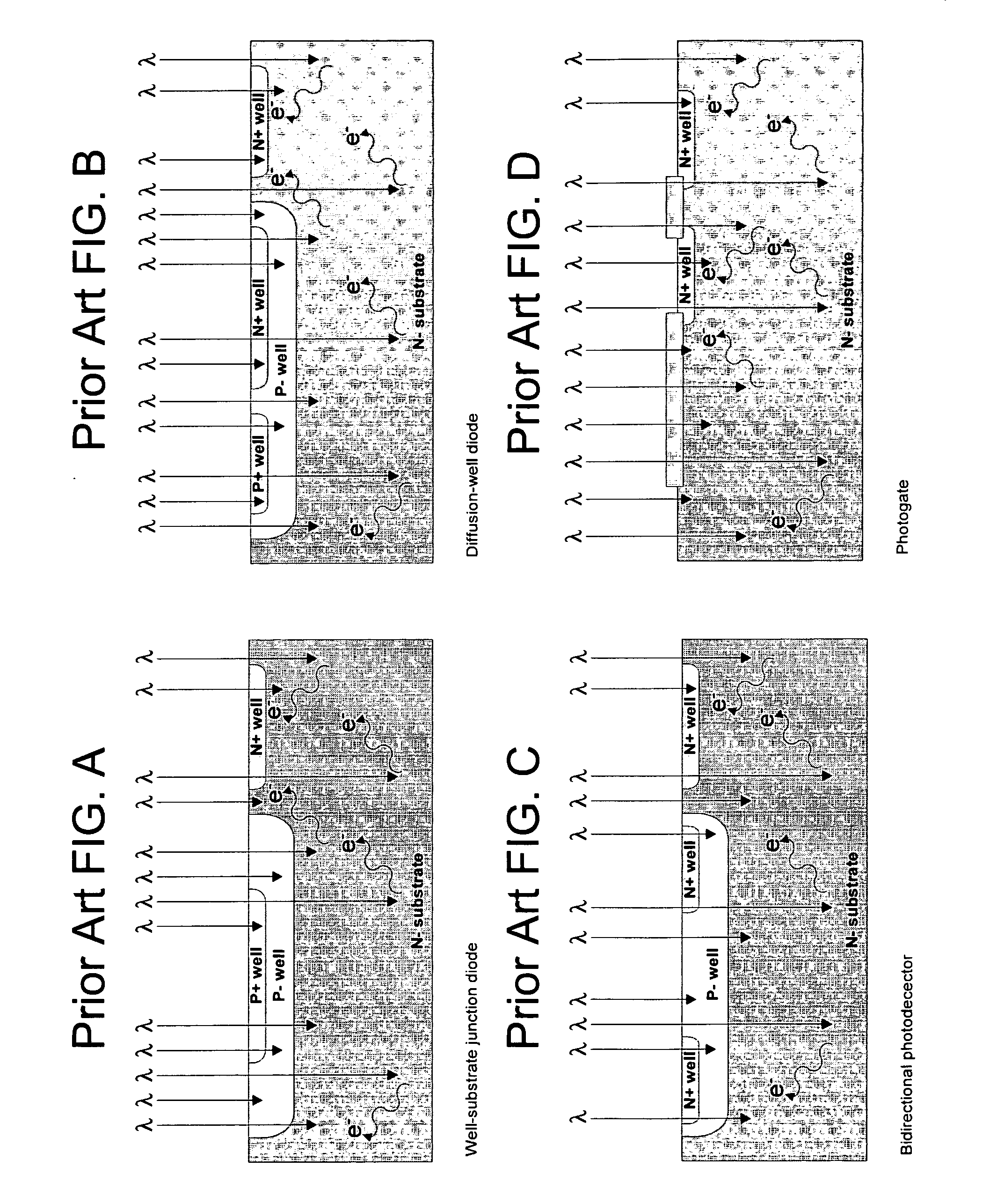
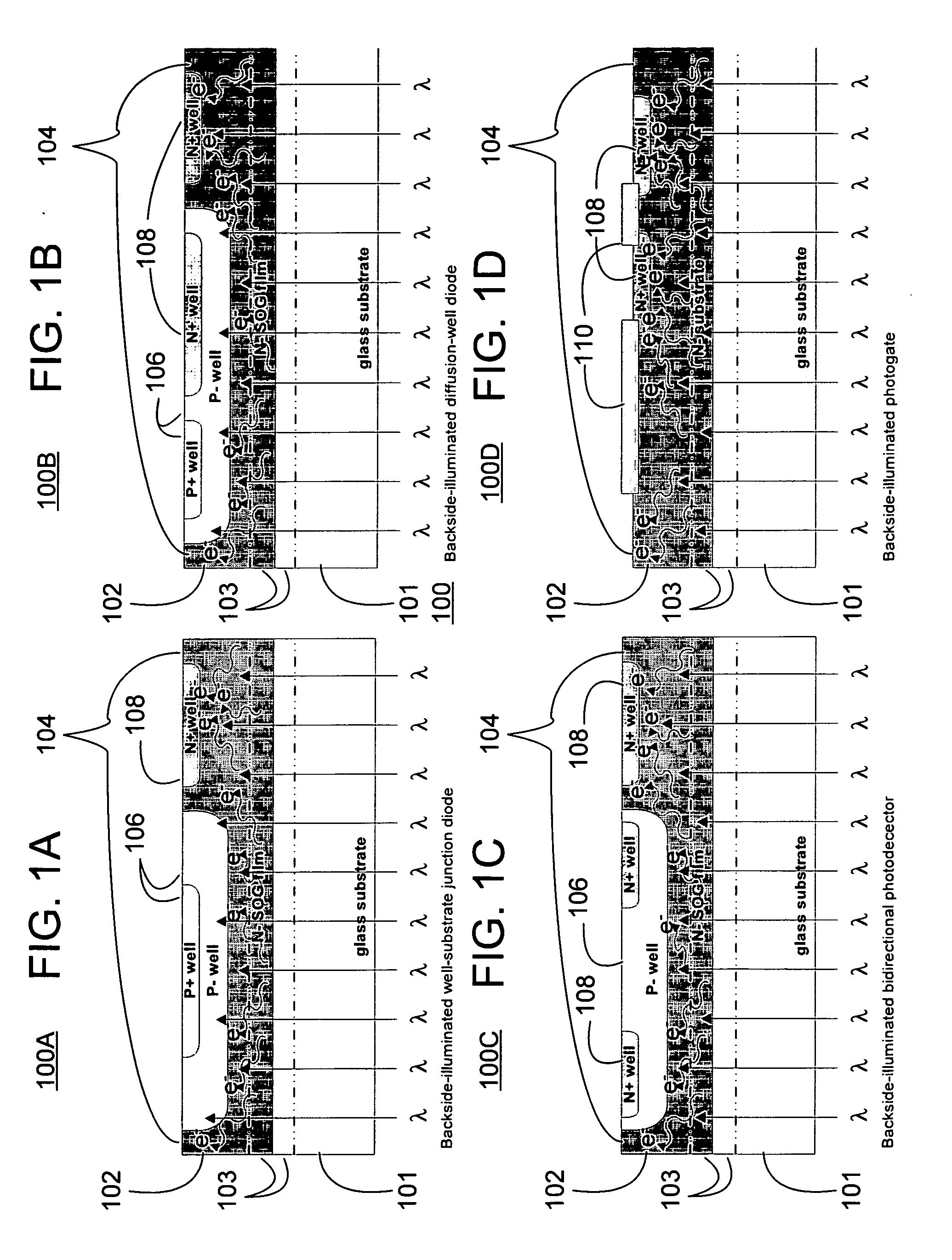
[0037]In particular, key advantages of preferred embodiments of the present invention include: 1) the use of low-cost, expansion-matched glass or glass ceramic substrates, compared to other more expensive semiconductor films (such as silicon, as has been used previously) or thermally mismatched ceramic substrates described in the prior art; 2) the presence of the single crystal template layer of Si, Ge or multilayer GaAs / Ge on the glass substrate, which is used as a template to create lattice matched, very low defect semiconductor layers for the image sensor features with high efficiencies, unlike polycrystalline templates used in prior art; 3) the transparency of the substrate allowing flexibility in module fabrication and utilization, including improved backside illumination and quantum efficiency; 4) the lack of adhesive between the glass and the rest of the image sensor (no interference, no instability, no added steps or cost, etc.); 5) mechanical durability of the image sensor due to protection offered by the glass substrate; 6) mechanical durability of the image sensor due to the strong anodic bond between the semiconductor film and the insulator substrate; and 7) design & fabrication flexibility to achieve image sensor structures that were previously impractical or impossible.

Problems solved by technology

The primary issues with the use of bulk Si are the cost and supply of high grade silicon and its utilization.
However, poly-crystalline silicon is disadvantageous for image sensors.
With a typical bulk crystal-Si or p-Si chip of 200 microns thick, the kerf loss from cutting wafers from boules or cast ingots is approximately 30%, significantly contributing to the overall cost.
Single crystalline wafers which are used in the semiconductor industry can be made into excellent image sensors, but expense is a major concern for large-scale mass production.
This can lead to reduced processing costs from that of bulk materials (in the case of silicon thin films) By contrast, manufacturing image sensors using wire-sawing bulk Si results in significant waste of prepared Si.
The former two methods, epitaxial growth and wafer-wafer bonding, have not resulted in satisfactory structures in terms of cost and / or bond strength and durability.
However, due to the high temperature steps, this process is not compatible with lower-cost glass or glass-ceramic substrates.

Method used


Image

  • Image sensor using thin-film SOI
  • Image sensor using thin-film SOI
  • Image sensor using thin-film SOI

Examples


Embodiment Construction

[0046]Image Sensor Types

[0047]Image sensors typically fall into one of two types: charge coupled devices (CCD) and active pixel sensors (APS) based on complementary-symmetry / metal-oxide semiconductor (CMOS) technology. A charge-coupled device (CCD) is an image sensor consisting of an integrated circuit containing an array of linked, or coupled, capacitors sensitive to light. Under the control of an external circuit, each capacitor can transfer its electric charge to one or other of its neighbors. Once the array has been exposed to the image, the control circuit causes each capacitor to transfer its contents to its neighbor. The last capacitor in the array dumps its charge into an amplifier that converts the charge into a voltage. By repeating this process, the control circuit converts the entire contents of the array to a varying voltage, which it samples, digitizes and stores in memory. Stored images can be transferred to a printer, storage device or video display.

[0048]The most co...


PUM


Abstract

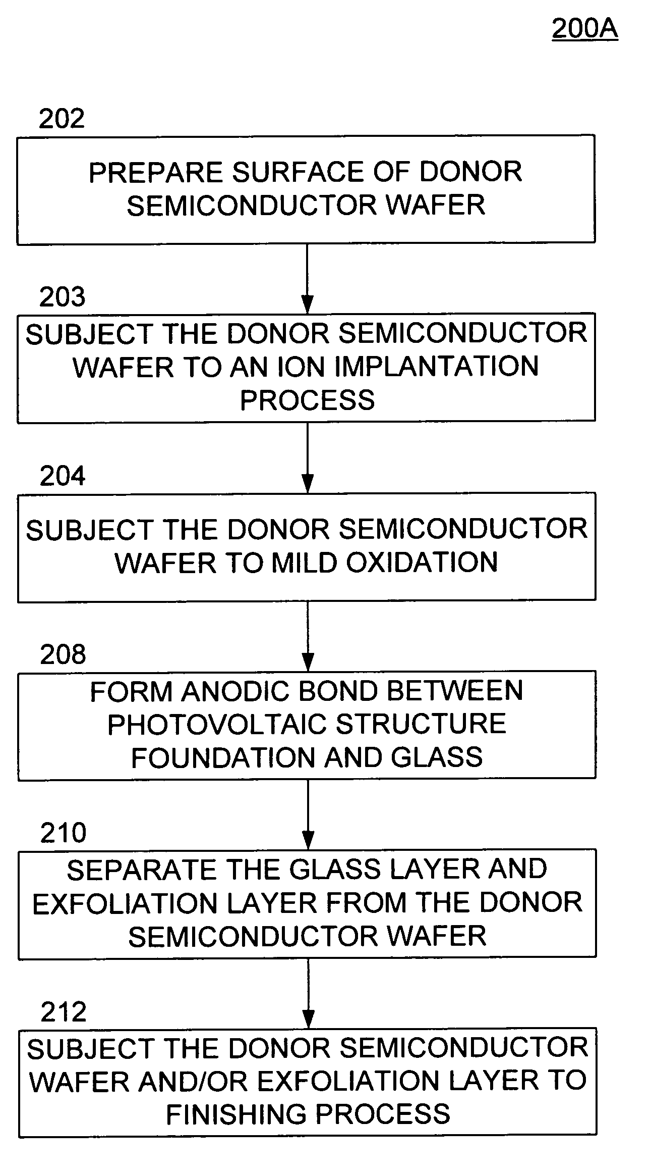
Systems and methods related to an image sensor of one or more embodiments include subjecting a donor semiconductor wafer to an ion implantation process to create an exfoliation layer of semiconductor film on the donor semiconductor wafer, forming an anodic bond between the exfoliation layer and an insulator substrate by means of electrolysis; separating the exfoliation layer from the donor semiconductor wafer to transfer the exfoliation layer to the insulator substrate; and creating a plurality of image sensor features proximate to the exfoliation layer. Forming the anodic bonding by electrolysis may include the application of heat, pressure and voltage to the insulator structure and the exfoliation layer attached to the donor semiconductor wafer. Image sensor devices include an insulator structure, a semiconductor film, an anodic bond between them, and a plurality of image sensor features. The semiconductor film preferably comprises an exfoliation layer of a substantially single-crystal donor semiconductor wafer.

Description

BACKGROUND[0001]1. Field of Invention[0002]The present invention relates to the systems, methods and apparatus relating to an image sensor, preferably having a substantially single crystal thin film, using improved processes, including in particular transferring and anodic bonding of a semiconductor layer to an insulator substrate.[0003]2. Description of Related Art[0004]Digital imaging has become a key technology in recent years with applications in consumer, industrial, scientific and medical imaging markets. Solid state image sensors are used in video cameras, X-ray equipment and scientific applications, such the Hubble telescope. The two main imaging technologies are based basically on the same principles, i.e., photovoltaic response of semiconductors when exposed to photons in the visible and near IR regions of the spectrum. The number of electrons released is proportional to light intensity.[0005]Image sensors are a specialized form of semiconductor structure, such as a semico...

Claims


Application Information

Patent Timeline
IPC IPC(8): H01L21/00
CPCH01L21/76254H01L27/1464H01L27/14692H01L27/14618H01L2924/0002H01L2924/00H01L21/762H01L27/146
Inventor BORRELLI, NICHOLAS FRANCISBRADY, MICHAEL DONAVONBURT, RONALD LEEGADKAREE, KISHOR PURUSHOTTAM
Owner CORNING INC
Learn More