
Gan-Based Field Effect Transistor and Production Method Therefor

a field effect transistor and transistor technology, applied in the field of field effect transistors, can solve the problems of reduced polarization effect at the heterointerface, increased resistance of the channel, reduced two-dimensional electron density, etc., and achieves small dispersion, small mobility, and a large increase in two-dimensional electron density.

Inactive Publication Date: 2007-12-27
NAT INST OF INFORMATION & COMM TECH
View PDF1 Cites 27 Cited by
  • Summary
  • Abstract
  • Description
  • Claims
  • Application Information

AI Technical Summary

Benefits of technology

[0059] Effects of the insulating film deposition in the AlGaN/GaN heterostructure FET according to the present invention will now be described.
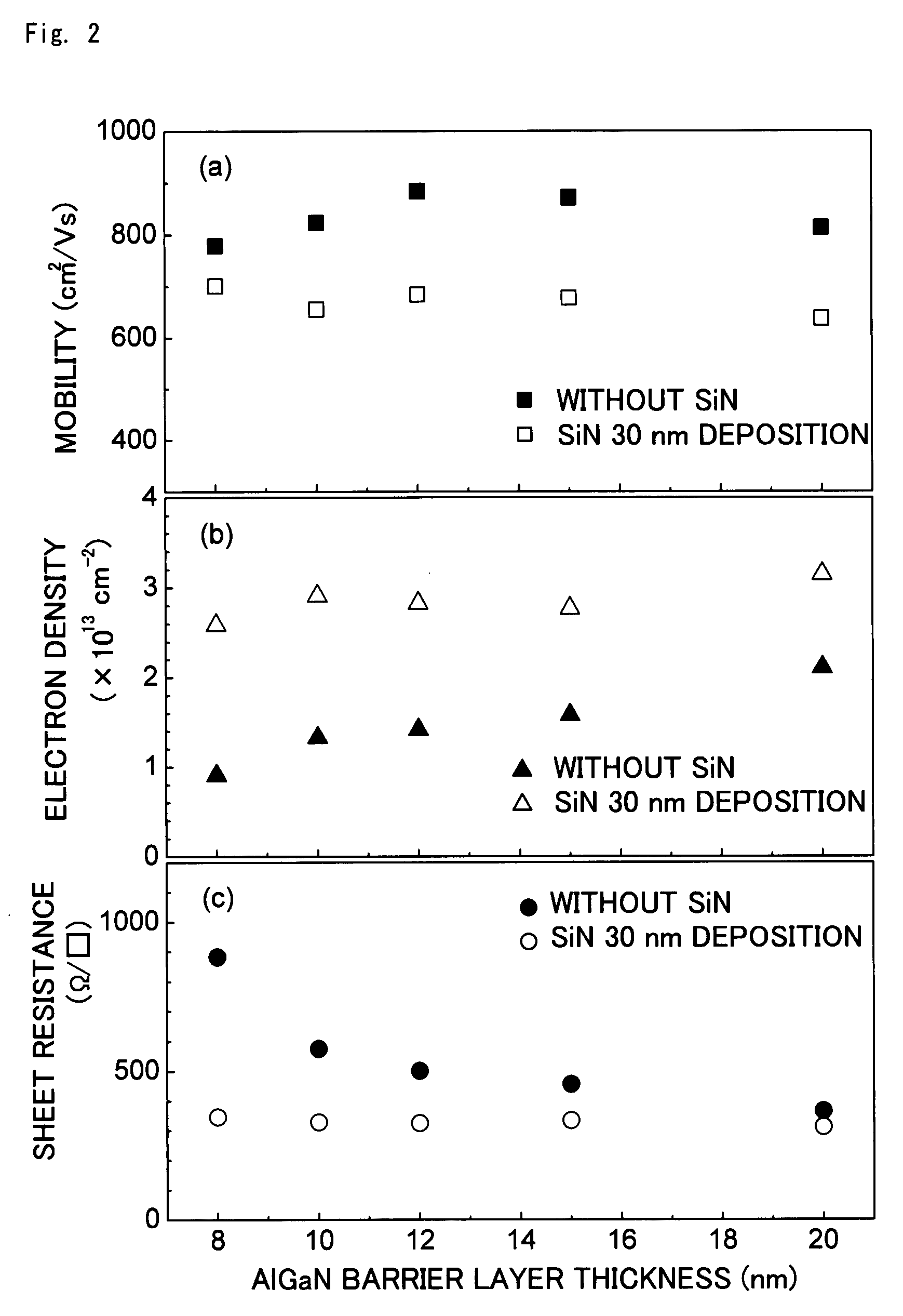
[0060] In FIG. 2, dependencies on the AlGaN barrier layer thickness for the electron mobility, the two-dimensional electron density, and the channel sheet resistance are plotted for Al0.4Ga0.6N/GaN heterostructure FETs having an Al04Ga0.6N barrier layer of a thickness from 8 to 20 nm with and without a 30-nm-thick SiN insulating film deposited on the AlGaN surface. FIG. 2(a) is a graph showing the electron mobility. In FIG. 2(a), blackened marks indicate ones without SiN insulating film deposition, while outlined marks indicate ones with 30 nm of the SiN insulating film deposition. Compared to the ones without the SiN insulating film, it is seen that the ones with the SiN insulating film deposited on the AlGaN surface have mobilities slightly reduced. However, it is seen that for ones with the SiN insulating film deposited on the AlGaN surface, the mobility when the film thickness of the AlGaN barrier layer changes to 8 nm-20 nm is almost constant as 640 cm2/Vs-700 cm2/Vs, and the dispersion is small.
[0061]FIG. 2(b) is a graph showing the two-dimensional electron density. In FIG. 2(b), blackened marks indicate ones without SiN insulating film deposition, while outlined marks indicate ones with 30 nm of the SiN insulating film deposition. It is seen from FIG. 2(b) that compared to the ones without the SiN insulating film, ones with the SiN insulating film deposited on the AlGaN surface have two-dimensional electron densities largely increased. Moreover, it is seen that for ones with the SiN insulating film deposited on the AlGaN surface, the values of the two-dimensional electron densities when the film thickness of the AlGaN barrier layer changes to 8 nm-20 nm are almost constant between 2.6×1013cm−2-3.2×1013 cm−2, and the dispersion is small. Also, it is seen that the thinner the film thickness...

Problems solved by technology

This brings problems that the polarization effect at the heterointerface is reduced, the two-dimensional electron density is reduced, and the resistance of the channel is increased.
However, since a gas ion etching is required in order to produce a recessed-gate FET, the process becomes complicated.
Also, since gas activated by plasma is used for etching, the etched semiconductor surface is damaged.
Also, since the reactive ion etching is not very accurate, it is difficult in reality to obtain appropriate recessed-gate FETs with a good reproducibility.

Method used


Image

  • Gan-Based Field Effect Transistor and Production Method Therefor
  • Gan-Based Field Effect Transistor and Production Method Therefor
  • Gan-Based Field Effect Transistor and Production Method Therefor

Examples


example 1

[0097] Hereinafter, an example of an AlGaN / GaN heterostructure FET on a sapphire substrate produced by the above-mentioned growth method for GaN-based compound semiconductors will be described.

[0098] A sapphire substrate was cleaned with organic solvent. The sapphire substrate, which had high melting point metal titanium evaporated on the back face in order to improve the heat-up capability of the substrate, was set at a substrate heater in the MBE growth chamber maintained at ultrahigh vacuum (e.g., 10−11 Torr-10−10 Torr). Then, the substrate was heated up to about 800 degrees C. and held at the temperature for 30 minutes for a high temperature cleaning of the substrate surface. Thereafter, the substrate temperature was lowered to 300 degrees C. Subsequently, nitrogen radicals obtained by decomposing nitrogen gas with the RF plasma were irradiated thereto. The sapphire substrate surface was nitrided for 60 minutes, and a thin aluminum nitride layer was formed on the surface.

[0099...

example 2

[0105] A heterostructure FET was produced with a similar process to the example 1 except that the AlGaN thickness was 18 nm. This heterostructure FET had a maximum drain current density of 725 mA / mm and a maximum transconductance of 190 mS / mm.

example 3

[0108] A heterostructure FET was produced by using the AlGaN film whose thickness is 10 nm, and with the same process as that of the example 1 until the preparation of the source and drain electrodes, whereafter the SiN insulating film was deposited for 2 nm, and a gate electrode with a further reduced length was prepared on the SiN insulating film by using electron beam lithography. Compared to the example 1, the gate electrode metal was changed from Ni / Au to Ti / Pt / Au, the source drain electrode spacing was changed from 5 μm to 2 μm, the gate length was changed from 1 μm to 0.06 μm, the gate width was changed from 50 μm to 100 μm. It is to be noted that while the gate electrode was prepared on the AlGaN barrier layer in the example 1, the gate electrode metal was prepared on the SiN insulating film in the example 3, so that a heterostructure FET with an MIS-gate structure as shown in FIG. 7 was obtained. This heterostructure FET had a maximum drain current density of 1.55 A / mm, a m...


PUM


Abstract

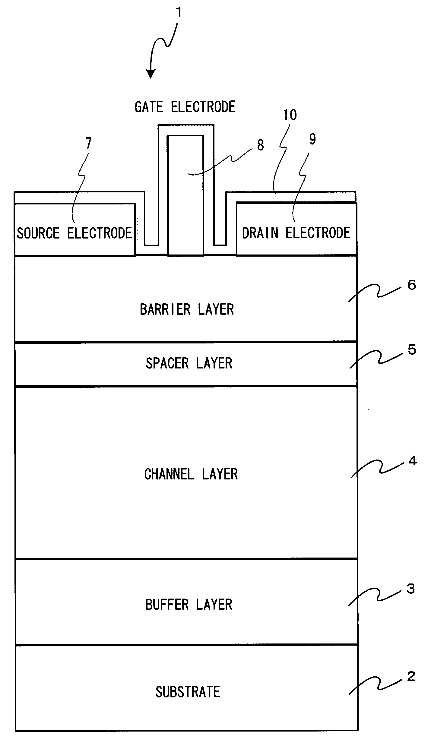
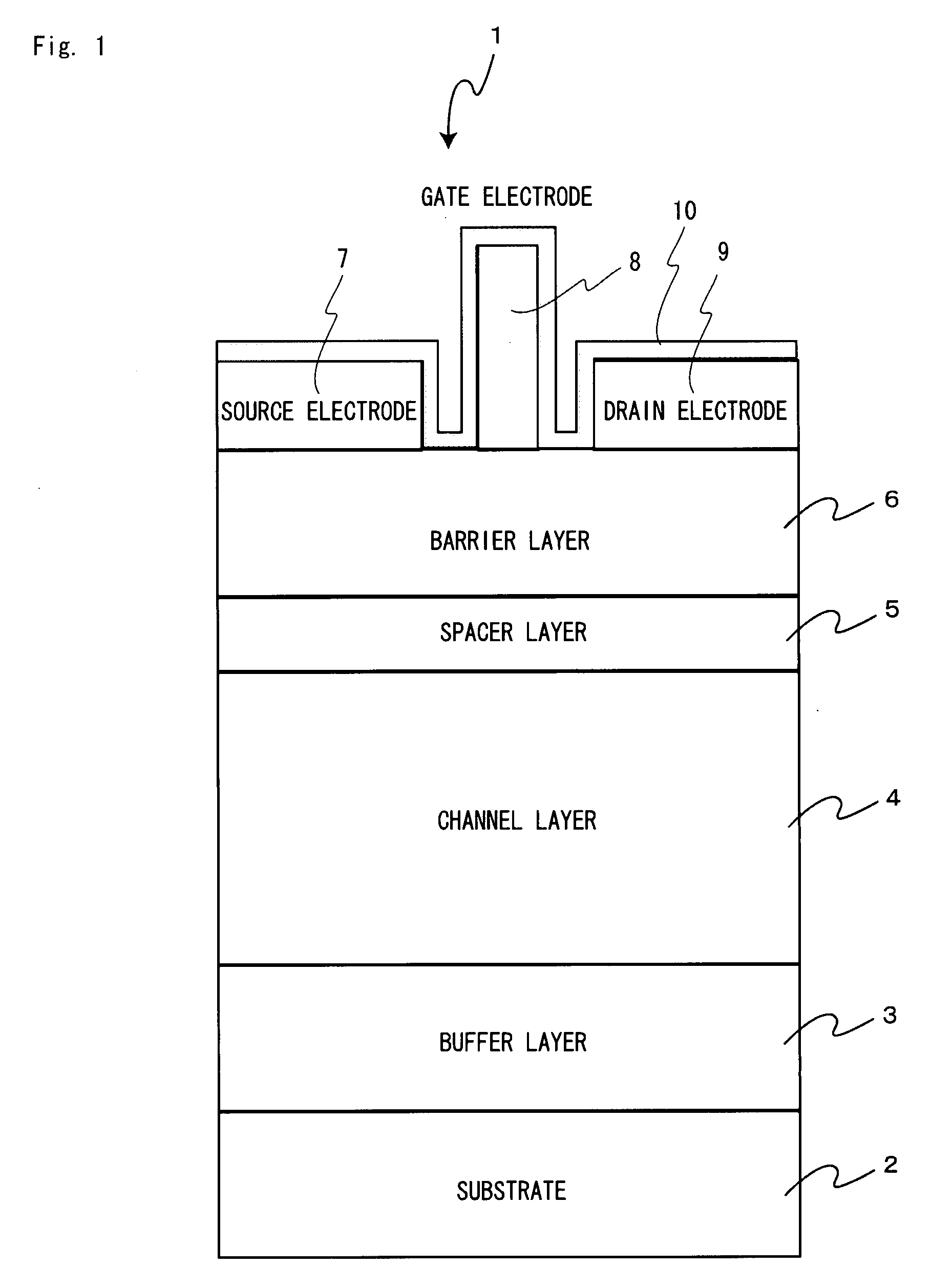
A GaN-based heterostructure field effect transistor capable of accomplishing higher output, higher breakdown voltage, higher speed, higher frequency, and the like. A heterostructure field effect transistor including a channel layer (4) of GaN and a barrier layer (6) of AlGaN, wherein the surface of a transistor element has an insulating film (10).

Description

TECHNICAL FIELD [0001] The present invention relates to a field-effect transistor having a heterostructure with a remarkable high output, high breakdown voltage, high speed, and high frequency response. BACKGROUND ART [0002] A heterostructure field-effect transistor (FET) is a transistor having an interface (heterointerface) consisting of two materials with different properties such as lattice constants, and two-dimensional electron gas formed at the heterointerface is made a channel. As a heterostructure FET, GaN-based FET is known. As the GaN-based FET, AlGaN / GaN heterostructure FET is known (see for example, following patent document 1 (Japanese Patent application laid-open No. 2003-258005), patent document 2 (Japanese patent application laid-open No. 2003-243424)). This AlGaN / GaN heterostructure FET can obtain a high two-dimensional electron density due to a polarization effect. FIG. 8 shows a schematic diagram of a general heterostructure FET. As shown in FIG. 8, the heterostru...

Claims


Application Information

Patent Timeline
IPC IPC(8): H01L21/338H01L29/778H01L29/812
CPCH01L29/0603H01L29/2003H01L29/812H01L29/66856H01L29/7786H01L29/66462
Inventor HIGASHIWAKI, MASATAKA
Owner NAT INST OF INFORMATION & COMM TECH
Learn More