Semiconductor wafer examination method and semiconductor chip manufacturing method

a semiconductor and wafer technology, applied in the direction of individual semiconductor device testing, semiconductor/solid-state device testing/measurement, instruments, etc., can solve the problems of failure of some semiconductor devices and semiconductor chips

Inactive Publication Date: 2007-11-01
SEIKO EPSON CORP
View PDF10 Cites 0 Cited by
  • Summary
  • Abstract
  • Description
  • Claims
  • Application Information

AI Technical Summary

Benefits of technology

[0006] An advantage of some aspects of the invention is to provide a semiconductor wafer examination method with which screening is performed at an earlier stage with high accuracy to find any possible failure.
[0009] With such a semiconductor wafer examination method according to some aspects of the invention, any failure that is highly likely to occur to a semiconductor wafer, e.g., at the time of semiconductor chip implementation, can be detected in advance so that screening can be performed with better reliability. This favorably leads to the reduction of failure occurrence so that the resulting semiconductor chip can be high in reliability.
[0015] With the semiconductor chip manufacturing method according to some aspects of the invention, the resulting semiconductor chip manufactured by such an examination method can be less likely to cause a failure.

Problems solved by technology

This thus may cause a failure to some semiconductor devices of the semiconductor chips if heat and pressure act on the electrodes of the semiconductor chips in the subsequent process of semiconductor chip implementation, for example.

Method used


Image

  • Semiconductor wafer examination method and semiconductor chip manufacturing method
  • Semiconductor wafer examination method and semiconductor chip manufacturing method
  • Semiconductor wafer examination method and semiconductor chip manufacturing method

Examples


Embodiment Construction

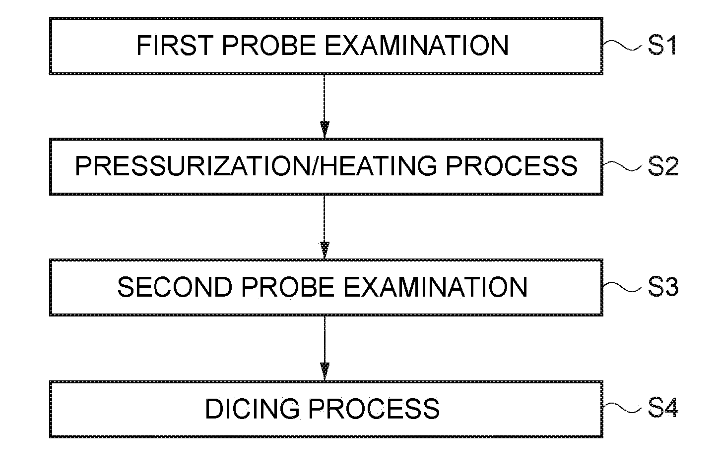
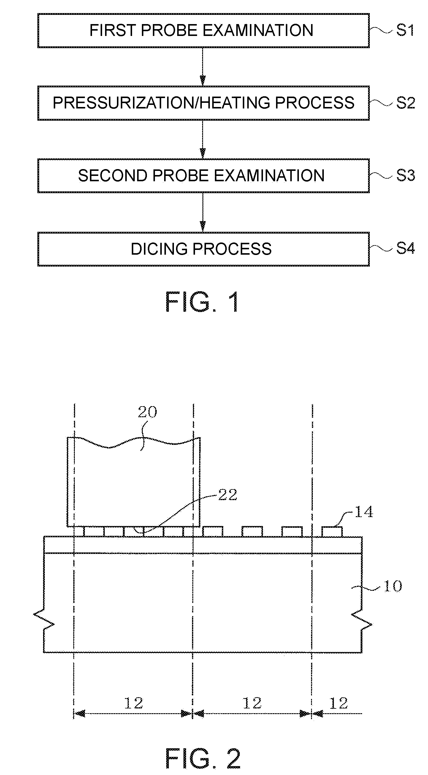
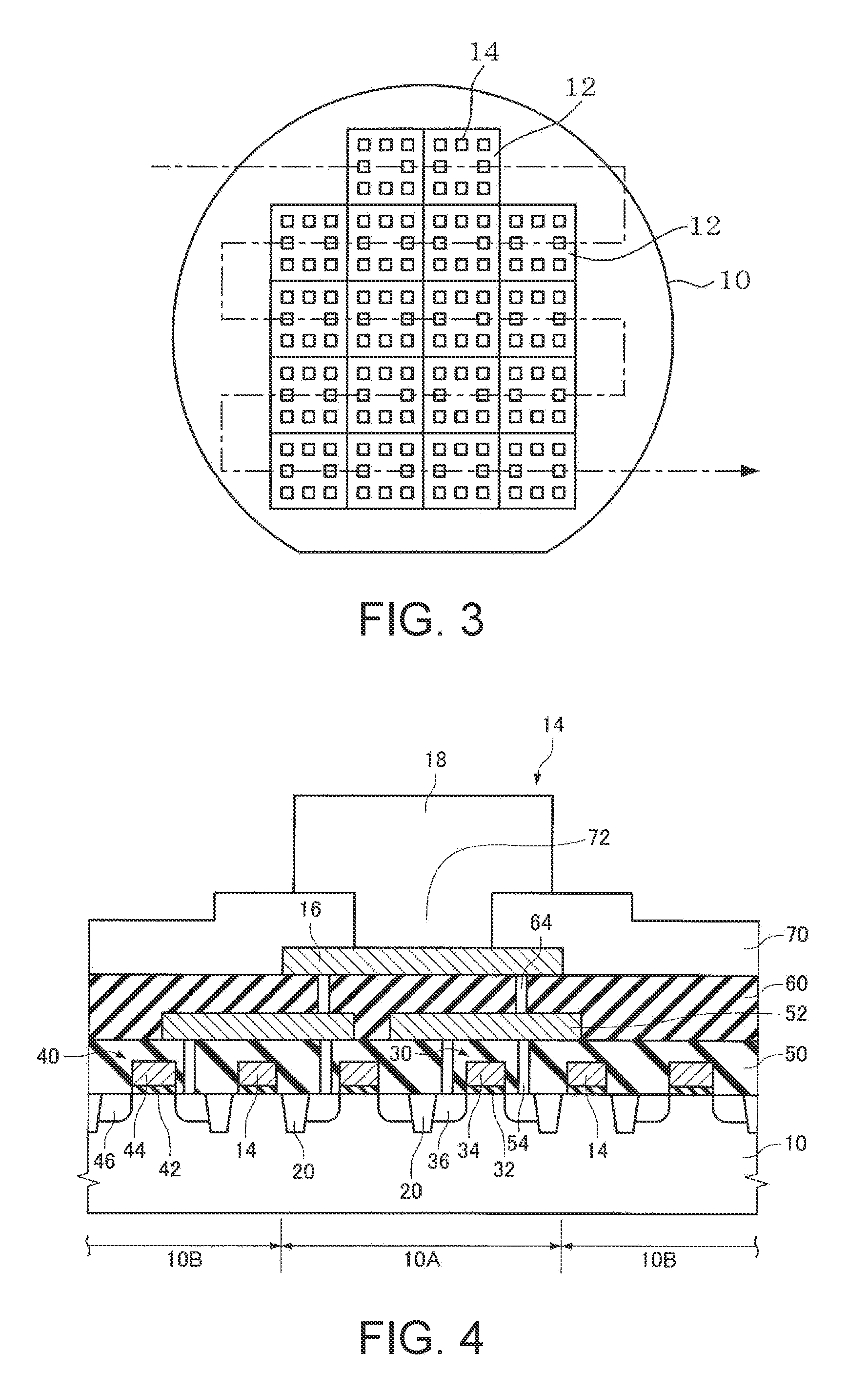
[0021] In the below, an exemplary embodiment of the invention is described by referring to the accompanying drawings. FIG. 1 is a diagram for illustrating a semiconductor wafer examination method of the embodiment. FIG. 2 is a cross sectional diagram schematically showing a process of the semiconductor wafer examination method. FIG. 3 is a schematic plan view of a wafer being an examination object. FIG. 4 is a schematic cross sectional view of a part of a chip area.

[0022] In the embodiment, a wafer is prepared for examination use. As shown in FIGS. 2 and 3, this wafer is configured by a semiconductor substrate 10 formed with a plurality of chip areas 12, which serve as semiconductor chips after wafer dicing. The chip areas 12 are provided with an integrated circuit that is not shown. The integrated circuit is not specifically defined by configuration, and may include an active element such as transistor or a passive element such as resistor, coil, or capacitor.

[0023] The chip area...


PUM


Abstract

A semiconductor wafer examination method that includes: preparing a wafer formed with a chip area for use as a semiconductor chip; firstly examining the wafer by probing; pressing an electrode of the wafer with a pressure member having a flat surface; and secondly examining the wafer by probing.

Description

CROSS-REFERENCE TO RELATED APPLICATIONS [0001] This application is a divisional of U.S. patent application Ser. No. 11 / 458,781 filed on Jul. 20, 2006, which claims the benefit of Japanese Patent Application No.2005-214218, filed Jul. 25, 2005. The disclosures of the above applications are incorporated herein by reference.BACKGROUND [0002] 1. Technical Field [0003] The present invention relates to a semiconductor wafer examination method by wafer probing, and a semiconductor chip manufacturing method. [0004] 2. Related Art [0005] In the process of manufacturing a semiconductor chip, a semiconductor wafer formed with a plurality of semiconductor chips is subjected to an electric examination on a semiconductor chip basis so that screening is performed to find any defective piece. Such an examination includes a probe examination by probing. After the wafer is subjected to the probe examination, the wafer is generally diced so that chips are formed. This thus may cause a failure to some ...

Claims


Application Information

Patent Timeline
Patent Type & Authority Applications(United States)
IPC IPC(8): H01L21/66
CPCG01R31/287H01L22/20G01R31/2881G01R31/2875
Inventor YUZAWA, HIDEKIKIJIMA, KAZUHIRO
Owner SEIKO EPSON CORP
Why Eureka
Try Eureka