
Devices and methods for constructing electrically programmable integrated fuses for low power applications

a technology of integrated fuse and electrical programming, which is applied in the direction of semiconductor devices, semiconductor/solid-state device details, instruments, etc., can solve the problems of reducing programming reliability, becoming more difficult to reliably blow fuses such as polysilicon fuses, etc., and achieves reliability and consistency, high efficiency, and high resistance.

Active Publication Date: 2007-11-01
INFINEON TECH AG +1
View PDF12 Cites 41 Cited by
  • Summary
  • Abstract
  • Description
  • Claims
  • Application Information

AI Technical Summary

Benefits of technology

[0006] In general, exemplary embodiments of the invention include electrically programmable polysilicon fuses that are designed for low power applications. More specifically, electrically programmable polysilicon fuses according to exemplary embodiments of the invention include stacked structures having conductive layers formed on polysilicon layers, which are designed to provide localized regions of high resistance in which fuse events can be localized and readily initiated using low programming current and voltages to achieve fuse programming with high efficiency, reliability and consistency.
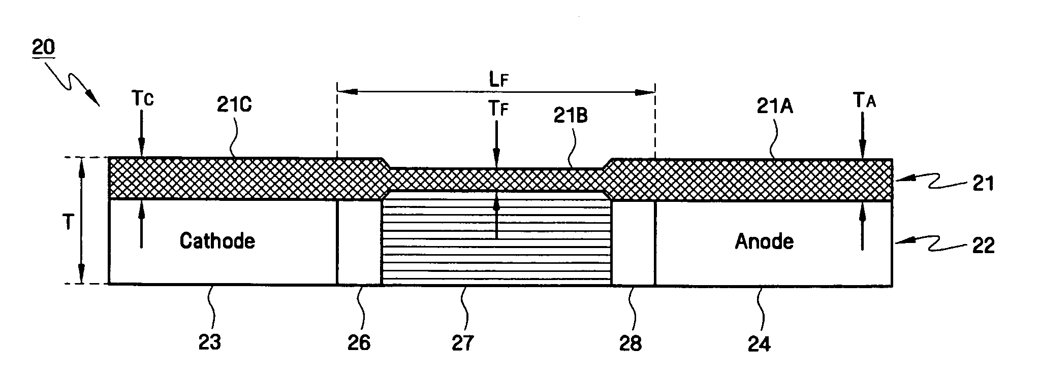
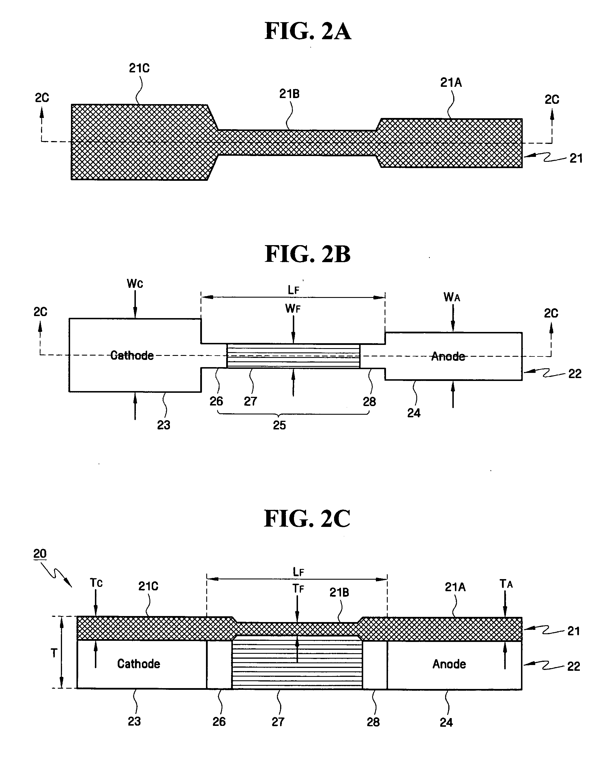
[0007] In one exemplary embodiment of the invention, a semiconductor integrated fuse includes a polysilicon layer comprising an anode, a cathode, a fuse link connected between the anode and cathode, and a conductive layer formed on the polysilicon layer. A first portion of the conductive layer formed over the fuse link has a first thickness T1 and a second portion of the conductive layer formed over the fuse link has a second thickness T2, where T2 is formed to be less than T1. The reduced thickness T2 of the second portion of the conductive layer provides a localized region of increased resistance in which a fusing event (e.g., melt or blow open the conductive layer) can be readily initiated by thermal stress generated with reduced currents / voltages to program the integrated fuse device.
[0009] In other exemplary embodiments of the invention, the doping profile of the polysilicon layer is varied over different regions of the polysilicon layer as a means to control the amount (thickness) of silicide formation as well as increase the ability to localize fusing events and control pre / post fuse resistance for low power applications.
[0010] For instance, in one exemplary embodiment of the invention, a fuse link region of the polysilicon layer is formed with different poly regions, where at least one poly region is a doped, electrically neutral poly region. The doping inhibits silicide formation such that a silicide layer is formed on the electrically neutral region which is thinner (higher resistance) than the silicide layers formed on adjacent poly regions. Moreover, the poly region is electrically neutral to provide a high resistance region which, during a programming operation, causes electrons flowing in the polysilicon at the junction between the electrically neutral poly region and an adjacent poly region to flow into the thin silicide layer, thereby increasing the vertical crowding and material migration in a manner which increases localization of thermal stress and enables more control to localize fusing events.

Problems solved by technology

With smaller voltages / currents, however, it becomes more difficult to reliably blow fuses such as polysilicon fuses.
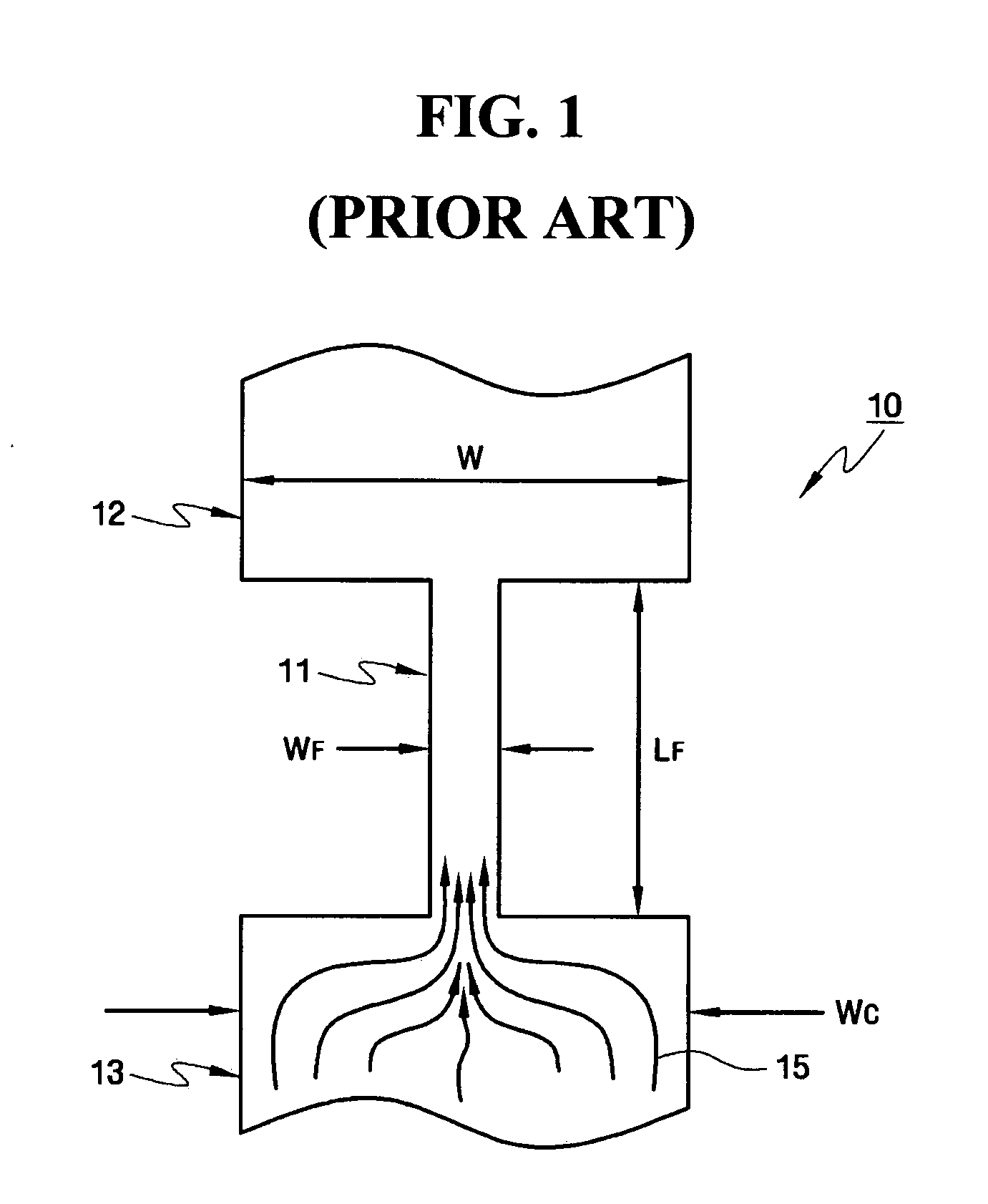
Although this design generally allows for programming with reduced current / voltage, the fusing location can vary across fuses of similar structure, thus reducing programming reliability.

Method used


Image

  • Devices and methods for constructing electrically programmable integrated fuses for low power applications
  • Devices and methods for constructing electrically programmable integrated fuses for low power applications
  • Devices and methods for constructing electrically programmable integrated fuses for low power applications

Examples


Embodiment Construction

[0016]FIGS. 2A-2C, 3A-3B and 4A-4B schematically illustrate electrically programmable semiconductor integrated fuse structures according to exemplary embodiments of the invention, which are designed to provide programming efficiency and reliability for low power applications. In general, FIGS. 2A-2C, 3A-3B and 4A-4B depict integrated fuses having stacked structures that commonly include a conductive layer (e.g., silicide layer) formed on top of a polysilicon fuse layer having anode and cathode regions and a fuse link region connecting the anode and cathode regions.

[0017] The exemplary integrated fuse structures are electrically programmed by applying a programming current of sufficient magnitude to create a current stress that increases the fuse temperature and initiates agglomeration of the fuse conductive layer which results in a fusing event that programs the fuse into a high resistance state. The fusing event may be formation of discontinuities or voids at a fusing location of ...


PUM


Abstract

Electrically programmable integrated fuses are provided for low power applications. Integrated fuse devices have stacked structures with a polysilicon layer and a conductive layer formed on the polysilicon layer. The integrated fuses have structural features that enable the fuses to be reliably and efficiently programmed using low programming currents / voltages, while achieving consistency in fusing locations. For example, programming reliability and consistency is achieved by forming the conductive layers with varied thickness and forming the polysilicon layers with varied doping profiles, to provide more precise localized regions in which fusing events readily occur.

Description

TECHNICAL FIELD OF THE INVENTION [0001] The present invention relates to programmable solid-state fuses and, more specifically, to electrically programmable polysilicon fuses that are designed for low power applications, as well as methods for constructing polysilicon fuses that can be reliably and efficiently programmed using low programming currents / voltages. BACKGROUND [0002] Semiconductor integrated fuses are utilized in various types of integrated circuit designs and applications. For instance, integrated fuses are utilized as programmable elements with memory devices (e.g., PROMs, SRAMs, etc.), redundancy for logic devices, programmable feature selection, etc. An integrated fuse can be programmed from a low resistance state to a high resistance state by applying an electric current of sufficient magnitude, and for a sufficient amount of time, to thereby heat the fuse to cause a fusing event (i.e., blow the fuse). [0003] Currently, integrated circuit devices are being developed...

Claims


Application Information

Patent Timeline
IPC IPC(8): H01L29/00
CPCH01L23/5256H01L2924/3011H01L2924/0002H01L2924/00H01L21/82H01L23/62
Inventor KO, YOUNG-GUNKU, JA-HUMSUN, MINCHULWEISER, ROBERT
Owner INFINEON TECH AG
Learn More