
Multimode focal plane array with electrically isolated commons for independent sub-array biasing

a focal plane array and sub-array biasing technology, applied in the field of multi-mode focal plane arrays, can solve the problems of not being able to meet the typical “active-passive” sensing application, requiring both high gain and temporally varying detector bias, and neither approach is suitable for typical “active-passive” sensing applications. , to achieve the effect of improving the fill-factor

Inactive Publication Date: 2007-04-05
TELEDYNE SCI & IMAGING
View PDF9 Cites 94 Cited by
  • Summary
  • Abstract
  • Description
  • Claims
  • Application Information

AI Technical Summary

Benefits of technology

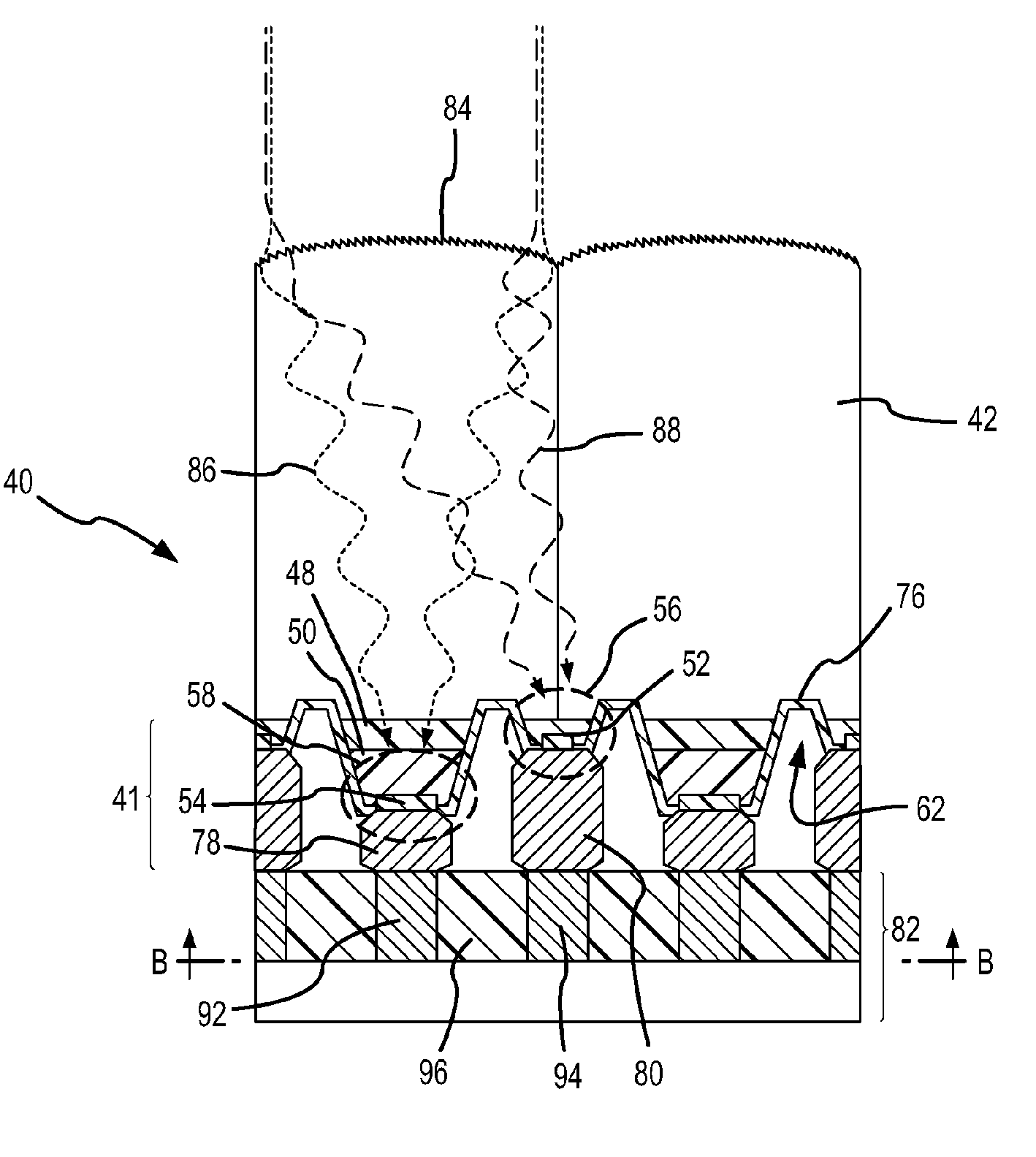
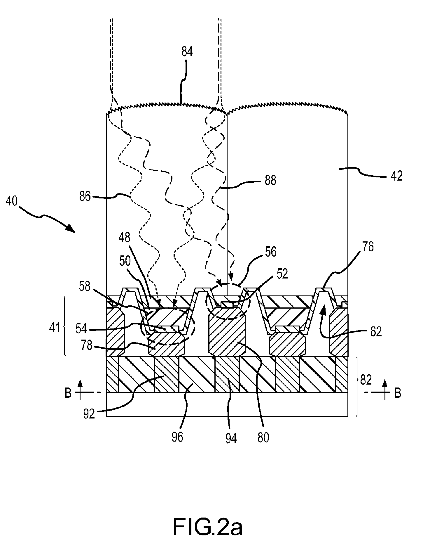
[0012] All of the detector array's conducting layers, including all of the absorbing layers, are patterned to form the electrically isolated commons for at least two, and in some instances all of the sub-arrays. Because the commons are electrically isolated, the application of substantially different bias voltages, in amplitude and / or temporal profile, does not produce crosstalk between the sub-arrays. The signal-to-noise ratio (SNR) is the most important figure of merit of a detector. Because of the isolated commons, the SNR of detectors in one sub-array is independent of the bias applied to another sub-array. Independent biasability allows the detector array to include APDs, PDs, PINs, photo capacitors, photo conductors or any combination thereof among the different sub-arrays to support different methods of detection including the “Active-Passive” case and improved sensitivity to incident radiation.
[0017] In another embodiment, in which the modes are determined, at least in part, by wavelength, external optics collect the incident radiation and focus it at an image plane above the FPA. Pixelated internal optics at this image plane separates the incident radiation within each pixel into different wavelengths and focuses the different wavelengths onto the appropriate photodetector sub-pixels in the respective sub-arrays. Each pixel of the internal optics typically uses a diffraction grating to separate the wavelengths and a refractive lens to focus them onto the photodetectors. The diffraction grating and refractive lens are suitably integrated into a unitary microlens. The use of such internal optics improves fill-factor by directing a larger portion of the incident radiation to the appropriate detectors and makes possible the use of single-layer FPAs by performing the wavelength selection optically.

Problems solved by technology

Although adequate for certain multi-spectral applications, neither approach is suitable for typical “Active-Passive” sensing applications.
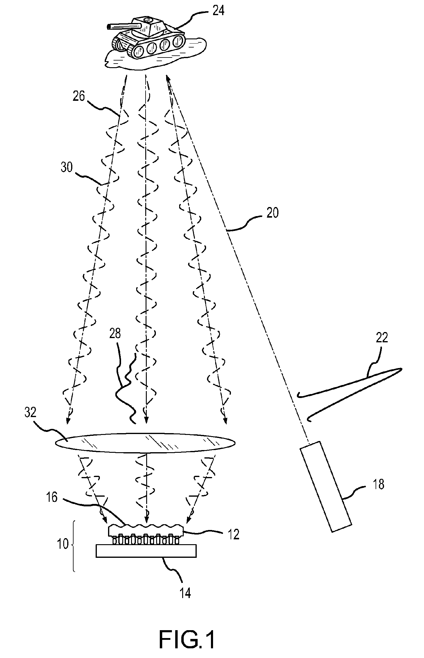
Due to the long distances from the source to the object and back to the detector, such active radiation is typically very dim (often only a few photons per sensing period per pixel) and often requires a very sensitive detector such as an avalanche photodiode or APD which has built-in gain that multiplies the photogenerated charge.
Moreover, some “lactive” signals are generated by pulsed or time-varying lasers and require both high gain and temporally varying detector bias.
Clearly, these bias voltages are not supported within the ranges of current CMOS design rules.
This system is large, heavy, expensive, and provides relatively poor registration.
If the voltage swings are extreme, however, the temporal swings may produce changes in neighboring pixels through stray capacitance or through spreading resistance flows that could change biases on neighboring detectors and produce cross-talk.

Method used


Image

  • Multimode focal plane array with electrically isolated commons for independent sub-array biasing
  • Multimode focal plane array with electrically isolated commons for independent sub-array biasing
  • Multimode focal plane array with electrically isolated commons for independent sub-array biasing

Examples


Embodiment Construction

[0028] The present invention provides an FPA that includes at least two sub-arrays of photodetectors for detecting incident radiation at different modes with elements of at least two sub-arrays co-located in each of at least one image pixel to provide registration among images from the different modes. The sub-arrays are configured with electrically isolated commons to support independent mode biasing.

[0029] The FPA may be configured to detect incident radiation over a broad spectrum including IR, visible, UV and possibly millimeter wave. The FPA can be constructed from any alloy semiconductor system with different band gaps, including the entire range of II-VI pseudobinary alloys (e.g. [Zn, Mn, Cd, Hg][S, Se, Te]), III-V pseudobinary alloys ([B, Al, Ga, ln][N, P, As, Si, Bi]), and IV-VI “lead salt” compounds ([Sn, Pb][S, Se, Te]). In addition, separate layers might be attached to one another by gluing and thinning while maintaining isolation between regions of common material used...


PUM


Abstract

In a multimode FPA, all of the FPA's conducting layers including all of the absorbing layers are patterned to form electrically isolated commons for at least two, and in some instances all of the photodetector sub-arrays, to support independent mode biasing of the photodetectors. Because the commons are electrically isolated, the bias voltages are not constrained by the CMOS design rules. The commons can accommodate large bias amplitude differences and different temporal bias profiles to address a wide range of multimode sensing applications.

Description

FIELD OF THE INVENTION [0001] This invention relates to multimode focal plane arrays (FPAs) formed with CMOS and semiconductor photodetector technologies and more specifically to a multimode FPA architecture with electrically isolated commons for independent sub-array biasing to accommodate large bias amplitude differences and different temporal bias profiles. DESCRIPTION OF THE RELATED ART [0002] A typical focal plane array (FPA) fabricated using CMOS and semiconductor photodetector technologies includes a layer of semiconductor material, suitably HgCdTe, that absorbs radiation over a broad spectral band such as infrared (IR), in the process generating electrical carriers (electrons or holes) within the material. The layer is selectively doped to form an array of photodetectors. A bias voltage is applied to the layer via a shared common so that the photodetectors can transfer the electrical carriers generated by the incident photons into a pixilated image pattern of electrical curr...

Claims


Application Information

Patent Timeline
IPC IPC(8): G11C16/04
CPCH01L27/14603H01L27/14609H01L27/14627H01L27/1465H01L27/1469H01L27/14696
Inventor TENNANT, WILLIAM E.
Owner TELEDYNE SCI & IMAGING
Learn More