
Source transistor configurations and control methods

a source transistor and control method technology, applied in the field of integrated circuits, can solve the problems of slow recovery, improper control of source transistors, chip operating delays, etc., and achieve the effects of reducing leakage, increasing the speed of integrated circuits, and reducing leakag

Inactive Publication Date: 2007-03-22
ZMOS TECH
View PDF14 Cites 33 Cited by
  • Summary
  • Abstract
  • Description
  • Claims
  • Application Information

AI Technical Summary

Benefits of technology

[0015] Circuits and methods are described for reducing leakage and increasing the speed of integrated circuits based on source transistor configurations and control methods. Configurations of stacked transistors provide source control and reduce leakage in standby modes while speeding discharge in active modes.
[0017] Another aspect of the invention is to provide fast virtual power recovery within circuit configuration and methods.
[0018] Another aspect of the invention is to provide fast recovery of virtual power line levels.
[0019] Another aspect of the invention is to provide self-reverse biasing techniques in combination with circuit to reduce leakage currents.

Problems solved by technology

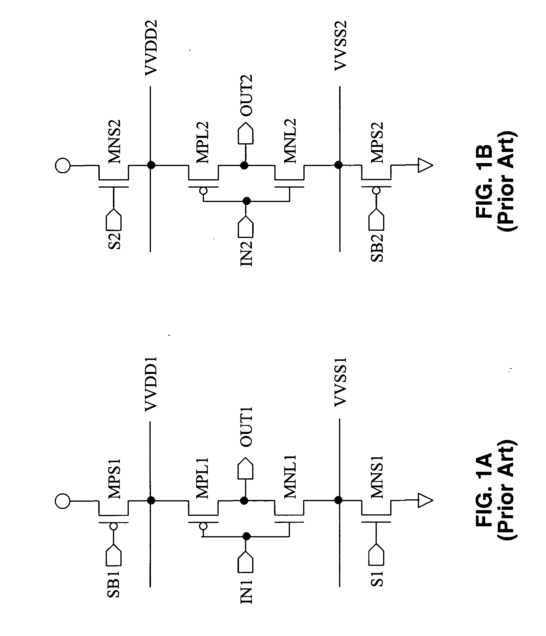
One issue that arises for leakage suppression techniques in source transistors is fast recovery of the virtual power line level, when the chip is changed into active mode from standby mode, so as not to incur additional delay in chip operation.
Other issues also arise in how to properly control source transistors according to their chip operating modes.
In consequence to this delay in turning on the source transistor, additional power line recovery time can be required that leads to chip operating delays.

Method used


Image

  • Source transistor configurations and control methods
  • Source transistor configurations and control methods
  • Source transistor configurations and control methods

Examples


Embodiment Construction

[0042] Referring more specifically to the drawings, for illustrative purposes the present invention is embodied in the apparatus generally shown in FIG. 3 through FIG. 20C. It will be appreciated that the apparatus may vary as to configuration and as to details of the parts, and that the method may vary as to the specific steps and sequence, without departing from the basic concepts as disclosed herein.

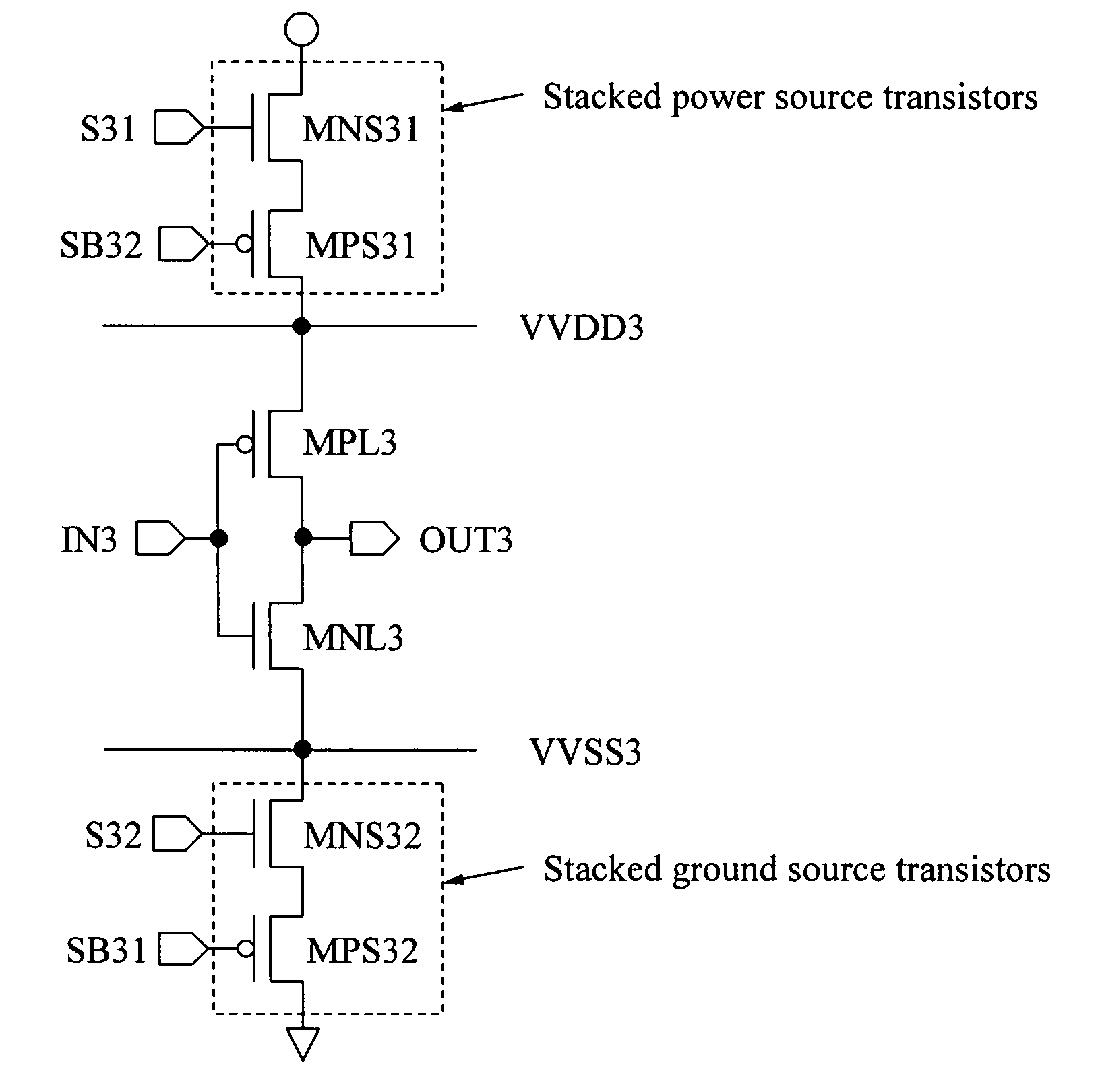
[0043]FIG. 3 illustrates an embodiment of a source transistor circuit configuration and method according to an aspect of the present invention for addressing the slow power line recovery time of the power line level. An embodiment of this configuration is composed of stacked source transistors such as transistors MNS31 and MPS31, as well as transistors MNS32 and MPS32.

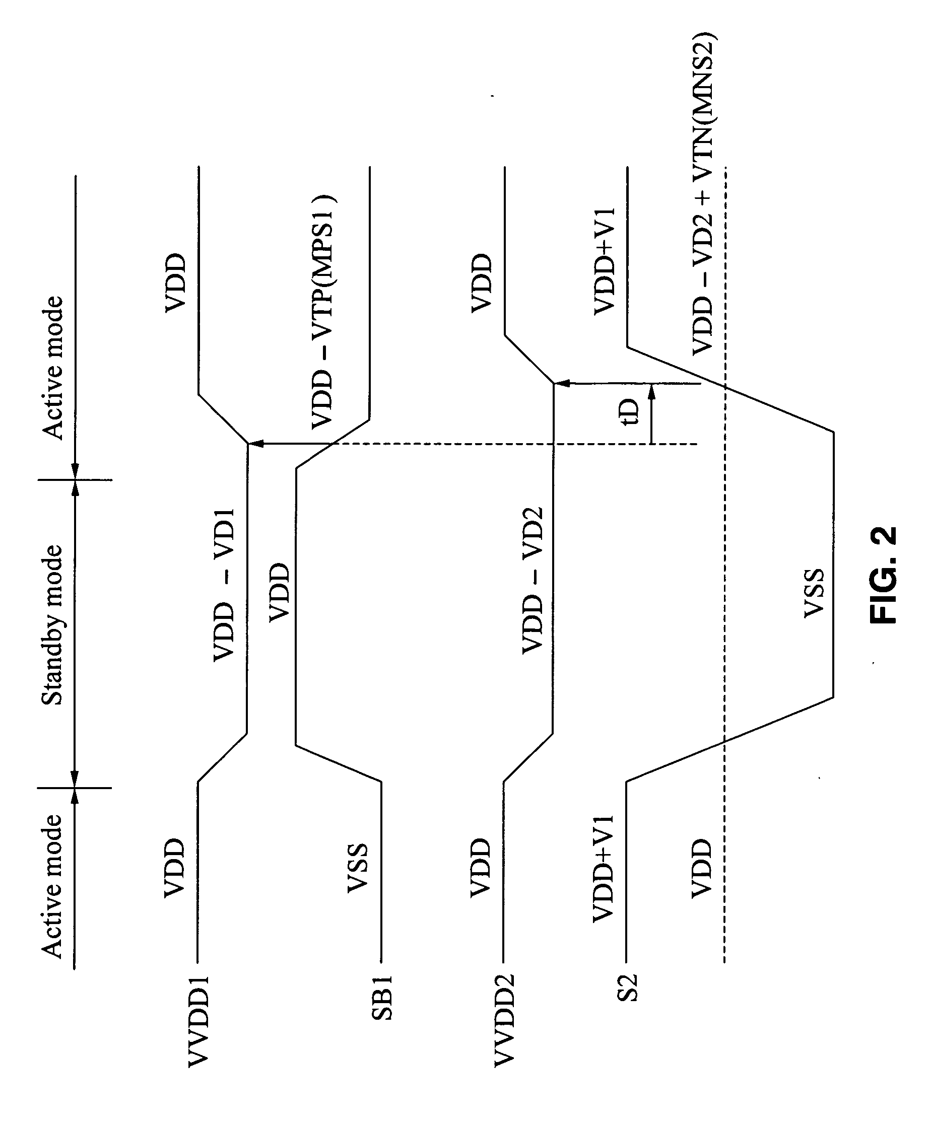
[0044]FIG. 4 illustrates control signal and node voltage levels of the proposed circuit for different operating modes. In active mode, in order to transfer the full VDD and VSS level without any Vt voltage drop gate si...


PUM


Abstract

Source transistor configurations are described for reducing leakage and delay within integrated circuits. Virtual power and ground nodes are supported with the use of stacked transistor configurations, such as a two transistor stack between a first virtual supply connection and VSS, and a second virtual supply connection and VDD. Gate drives of these stacked transistors are modulated with different voltage levels in response to the operating power mode of the circuit, for example active mode, active-standby mode, and deep power-down mode. Means for driving these source stacks are described. In one embodiment separate virtual nodes are adapted for different types of circuits, such as buffers, row address strobe, and column address strobe. Other techniques, such as directional placement of the transistors is also described.

Description

CROSS-REFERENCE TO RELATED APPLICATIONS [0001] This application claims priority from U.S. provisional application Ser. No. 60 / 697,672 filed on Jul. 8, 2005, which is incorporated by reference herein in its entirety.STATEMENT REGARDING FEDERALLY SPONSORED RESEARCH OR DEVELOPMENT [0002] Not Applicable INCORPORATION-BY-REFERENCE OF MATERIAL SUBMITTED ON A COMPACT DISC [0003] Not Applicable NOTICE OF MATERIAL SUBJECT TO COPYRIGHT PROTECTION [0004] A portion of the material in this patent document is subject to copyright protection under the copyright laws of the United States and of other countries. The owner of the copyright rights has no objection to the facsimile reproduction by anyone of the patent document or the patent disclosure, as it appears in the United States Patent and Trademark Office publicly available file or records, but otherwise reserves all copyright rights whatsoever. The copyright owner does not hereby waive any of its rights to have this patent document maintained...

Claims


Application Information

Patent Timeline
Patent Type & Authority Applications(United States)
IPC IPC(8): G05F1/10
CPCG11C7/1045G11C11/4074H03K19/0016G11C2207/2227G11C11/4076G05F1/10H01L29/00
Inventor YOO, SEUNG-MOONYOO, JAE HOONSOHN, JEONGDUKSON, SUNG JUCHOI, MYUNG CHANKIM, YOUNG TAEYOON, OH SANGHAN, SANG-KYUN
Owner ZMOS TECH
Learn More