
Method of fabricating metal-insulator-metal capacitor

a technology of metal-insulator and capacitor, which is applied in the direction of capacitors, basic electric elements, electrical equipment, etc., can solve the problems of deteriorating semiconductor device characteristics, the limit of the scaled-down dielectric layer in the high integration dram device, etc., and achieve the effect of improving electrical characteristics

Inactive Publication Date: 2007-02-01
SAMSUNG ELECTRONICS CO LTD
View PDF5 Cites 13 Cited by
  • Summary
  • Abstract
  • Description
  • Claims
  • Application Information

AI Technical Summary

Benefits of technology

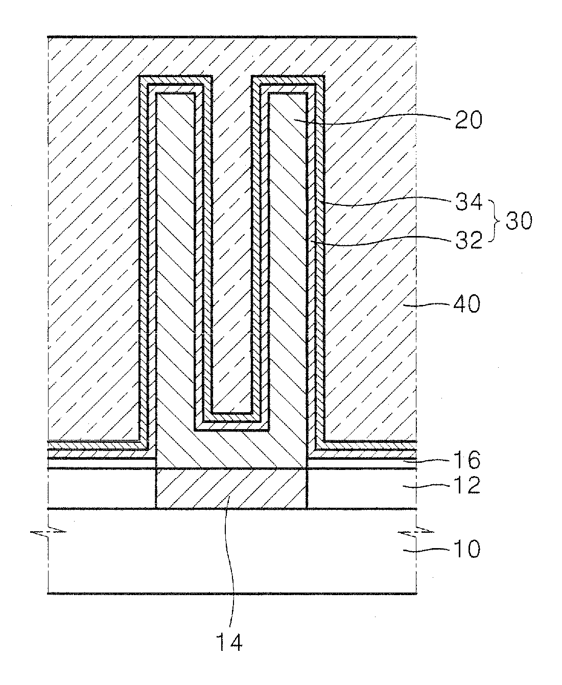
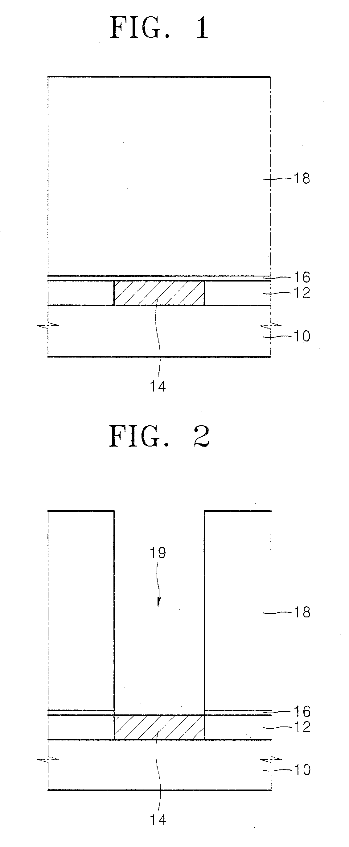
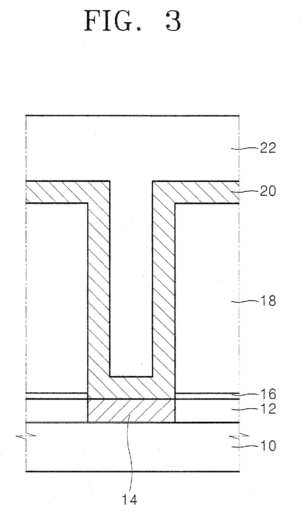
The present invention provides a method for making a metal-insulator-metal (MIM) capacitor with improved production and electrical characteristics. The method includes forming an interlayer insulating layer with a contact plug on a semiconductor substrate, adding an etch stop layer, creating a mold layer with an opening exposing the contact plug, adding a first conductive layer for a lower electrode, adding a photoresist layer, removing the mold layer and photoresist layer, and adding a composite dielectric layer on the lower electrode. A second conductive layer is then added on top of the composite dielectric layer. The composite dielectric layer is made of an oxide hafnium layer and an oxide aluminum layer, with the thickness of the oxide hafnium layer determined to achieve a predetermined capacitance of the capacitor. This method allows for improved production and electrical performance of the MIM capacitor.

Problems solved by technology

However, the dielectric layers have limits in how scaled down they can get in high integration DRAM devices.
Particularly, when HfO2 is used as a single layer, the characteristics of a semiconductor device are deteriorated due to the crystallization of HfO2.
However, since HfO2 has the problem of poor leakage current characteristics, and is crystallized as described above, it is limited in its use to fabricate a capacitor having excellent electrical characteristics.

Method used


Image

  • Method of fabricating metal-insulator-metal capacitor
  • Method of fabricating metal-insulator-metal capacitor
  • Method of fabricating metal-insulator-metal capacitor

Examples


experimental example 1

[0031] In order to examine the characteristics of the capacitor fabricated according to an embodiment of the present invention, in which an oxide hafnium dielectric layer and an oxide aluminum dielectric layer is formed, the leakage current characteristics of the MIM capacitor in accordance with the order formation of the dielectric layers is evaluated.

[0032] In the fabrication of the MIM capacitor according to this example, a 20 Å thick oxide hafnium dielectric layer is formed on a TiN lower electrode, a 40 Å thick oxide aluminum dielectric layer is formed on the oxide hafnium dielectric layer, and an upper electrode composed of TiN is formed on the resulting structure. The upper and lower electrodes are formed at a temperature of about 560° C. using an ALD method. The dielectric layers are deposited at a temperature of about 350° C. using an ALD method, in which O3 is used as an oxygen source gas. In a comparative example, upper and lower electrodes can be formed in the same mann...

experimental example 2

[0035] In this example, a MIM capacitor was fabricated by varying the thickness of an oxide hafnium dielectric layer in a same range of an equivalent oxide dielectric layer thickness and the leakage current characteristic of the MIM capacitor was evaluated.

[0036] The MIM capacitor of the present invention was fabricated in the same manner as that of the experiment example 1, in which an oxide hafnium dielectric layer of the MIM capacitor was formed with thicknesses of 20 Å, 40 Å, 45 Å, and 50 Å, respectively. An equivalent oxide dielectric layer thickness of 20 Å was used in order to compare the leakage current characteristics of the capacitor in a same range of an equivalent oxide dielectric layer thickness. Therefore, an oxide aluminum dielectric layer was formed with thicknesses of 32 Å, 24 Å, 22 Å, and 20 Å, respectively, which were achieved by subtracting a thickness of the oxide hafnium dielectric layer from the composite dielectric layer thickness corresponding to an equival...

experimental example 3

[0039] An oxide aluminum dielectric layer was deposited on an oxide hafnium dielectric layer, and the leakage current characteristics of a MIM capacitor were evaluated in accordance with the deposition temperature.

[0040] The MIM capacitor of the present invention was fabricated in the same manner as with experimental example 1, but the deposition temperature of the oxide aluminum dielectric layer was set to vary between about 300° C. and about 450° C.

[0041] Results of measuring a leakage current amount per cell of the semiconductor substrate in accordance with voltages applied to the capacitor are illustrated in FIG. 11. The deposition temperature of the capacitor represented by ‘g’ was set to about 450° C., and a deposition temperature of the capacitor represented by ‘h’ was set to about 300° C. In FIG. 11, it was acknowledged that the capacitor of ‘g’ showed less leakage current than the capacitor of ‘h’ at about 1.2 V. Hence, the leakage current of the MIM capacitor of the pres...


PUM


Abstract

In one embodiment, a method of fabricating a MIM capacitor includes forming an interlayer insulating layer having a contact plug on a semiconductor substrate, forming an etch stop layer on the interlayer insulating layer, and forming a mold layer having an opening exposing the contact plug on the etch stop layer. Next, a first conductive layer for the lower electrode is formed on the sidewalls and the bottom of the opening, and a photoresistive layer is formed on the first conductive layer. The mold layer and the photoresistive layer are then removed, and a composite dielectric layer is formed on the lower electrode. A second conductive layer is then formed on the composite dielectric layer. The composite dielectric layer may be composed of an oxide hafnium (HfO2) dielectric layer and an oxide aluminum (Al2O3) dielectric layer, with the oxide hafnium dielectric layer having a thickness of about 20 Å to about 50 Å. The oxide aluminum dielectric layer is formed with a thickness determined by subtracting the thickness of the oxide hafnium dielectric layer from a composite dielectric layer thickness corresponding to an equivalent oxide dielectric layer thickness set to provide a predetermined capacitance of the capacitor.

Description

CROSS-REFERENCE TO RELATED PATENT APPLICATION [0001] This application claims the benefit of Korean Patent Application No. 10-2005-0069139, filed on Jul. 28, 2005, in the Korean Intellectual Property Office, the disclosure of which is incorporated herein in its entirety by reference. BACKGROUND OF THE INVENTION [0002] 1. Field of the Invention [0003] The present invention relates to a method of fabricating a capacitor of a semiconductor device, and more particularly, to a method of fabricating a metal-insulator-metal (MIM) capacitor using metal oxide as a dielectric layer. [0004] 2. Description of the Related Art [0005] As the integration density of semiconductor devices is increased, capacitors in the semiconductor devices require a higher capacitance per unit area. The capacitance is inversely proportional to the distance between capacitor electrodes, and proportional to the permittivity and surface area of the electrode. Hence, in order to fabricate a capacitor having a high capac...

Claims


Application Information

Patent Timeline
Patent Type & Authority Applications(United States)
IPC IPC(8): H01L21/473H10B12/00
CPCH01L21/02178H01L21/02181H01L21/022H01L28/91H01L21/3142H01L21/3162H01L21/31645H01L21/0228H10B99/00
Inventor CHUNG, JUNG-HEELEE, JONG-CHEOLCHOI, JAE-HYOUNGCHOI, JEONG-SIKOH, SE-HOONYOO, CHA-YOUNG
Owner SAMSUNG ELECTRONICS CO LTD
Learn More