Heatsink films for magnetic recording media
a magnetic recording and film technology, applied in the field of heatsink films for magnetic recording media, can solve the problems of few hard magnetic materials, the recording head is not able to provide a sufficient magnetic writing field to write on such materials, and the conventional form of magnetic recording has been projected to suffer from superparamagnetic instabilities at high bit densities, etc., to achieve good mechanical properties, high hardness, and high thermal conductivity
- Summary
- Abstract
- Description
- Claims
- Application Information
AI Technical Summary
Benefits of technology
Problems solved by technology
Method used
Image
Examples
example 1
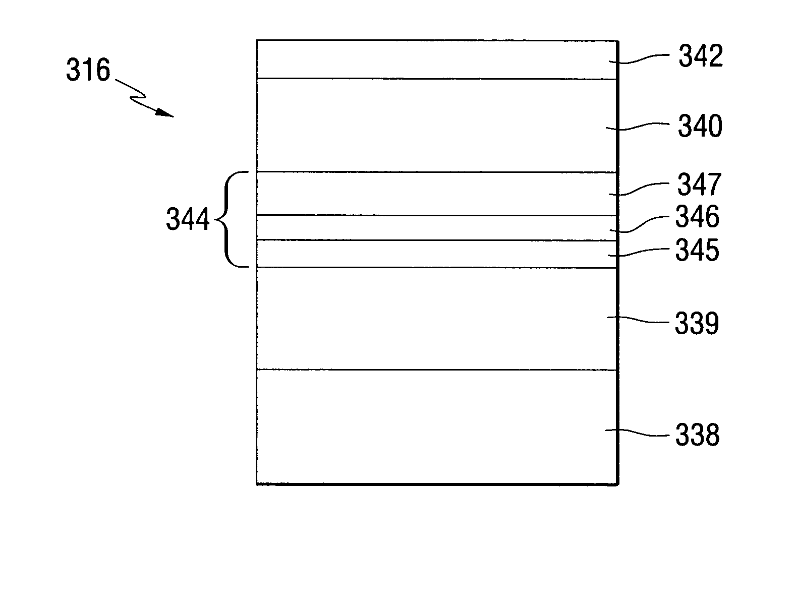
[0045] A technique known as the femtosecond (or ultrafast) pump probe method was used to evaluate thermal properties of different heatsink films. It is a combination of high temporal resolution provided by femtosecond lasers and high magnetic sensitivity offered by magneto-optical characterization techniques. In a pump-probe configuration, the equilibrium magnetization is perturbed by an intense pump (Ti: sapphire laser) pulse. The ultra-fast evolution of the distorted magnetic state is then monitored by a second probe (laser beam produced by the SHG generator) pulse. For the thermal conductivity measurement, the reflectivity change at the sample surface is monitored to compare the value expected from the theoretical value from the sample layer structure.
[0046]FIG. 7 presents the cooling speed dependence on the CuZr heatsink thickness in a sample similar to that shown in FIG. 5 measured by the pump probe method. The cooling speed decreases with the CuZr thickness, but no improvemen...
example 2
[0050]FIGS. 11a and 11b illustrate a scratch depth comparison between a relatively low hardness pure Cu film in comparison with a relatively high hardness CuZr film of the present invention. As shown in FIG. 11a, a pure Cu film subjected to the standard surface scratch test exhibits a scratch depth of approximately 3 to 5 nm. In FIG. 11b, the CuZr alloy film of the present invention exhibits a scratch depth of approximately 2 to 3 nm. FIG. 11b illustrates significant improvement in the mechanical hardness of the CuZr alloy film subjected to the surface scratch test under Atomic Force Microscope (AFM). The scratch depth at the CuZr film surface is about a half of those made on pure Cu surface. The surface scratch test is commonly conducted to test the compatibility of a material with the hard disc medium material and with the media fabrication process. Typical post sputtering processes including lubricant application, buff / wipe and glide testing can apply mechanical stress which may ...
PUM
| Property | Measurement | Unit |
|---|---|---|
| thickness | aaaaa | aaaaa |
| thickness | aaaaa | aaaaa |
| FWHM | aaaaa | aaaaa |
Abstract
Description
Claims
Application Information
 - R&D
- Intellectual Property
- Life Sciences
- Materials
- Tech Scout
- Unparalleled Data Quality
- Higher Quality Content
- 60% Fewer Hallucinations
Browse by: Latest US Patents, China's latest patents, Technical Efficacy Thesaurus, Application Domain, Technology Topic, Popular Technical Reports.
© 2025 PatSnap. All rights reserved.Legal|Privacy policy|Modern Slavery Act Transparency Statement|Sitemap|About US| Contact US: help@patsnap.com


