Method of manufacturing nitride semiconductor light emitting diode

Inactive Publication Date: 2006-10-19
SAMSUNG ELECTRO MECHANICS CO LTD
View PDF6 Cites 14 Cited by
  • Summary
  • Abstract
  • Description
  • Claims
  • Application Information

AI Technical Summary

Benefits of technology

[0014] The present invention has been made to solve the foregoing problems of the prior art and it is therefore an object of the present invention to provide a novel method of manufacturing a nitride semiconductor light emitting diode capable of establishing a superior ohmic contact without heat processing by directly depositing a nickel oxide to a thickness that ensures light transmissibility and combining the same with a light transmissible conductive oxide layer.

Problems solved by technology

Also, the thickness exceeding about 20 Å causes light loss to increases proportional to the thickness of the nickel oxide film, thereby hardly ensuring high brightness.

Method used


Image

  • Method of manufacturing nitride semiconductor light emitting diode
  • Method of manufacturing nitride semiconductor light emitting diode
  • Method of manufacturing nitride semiconductor light emitting diode

Examples


Embodiment Construction

[0025] Preferred embodiments of the present invention will now be described in detail with reference to the accompanying drawings.

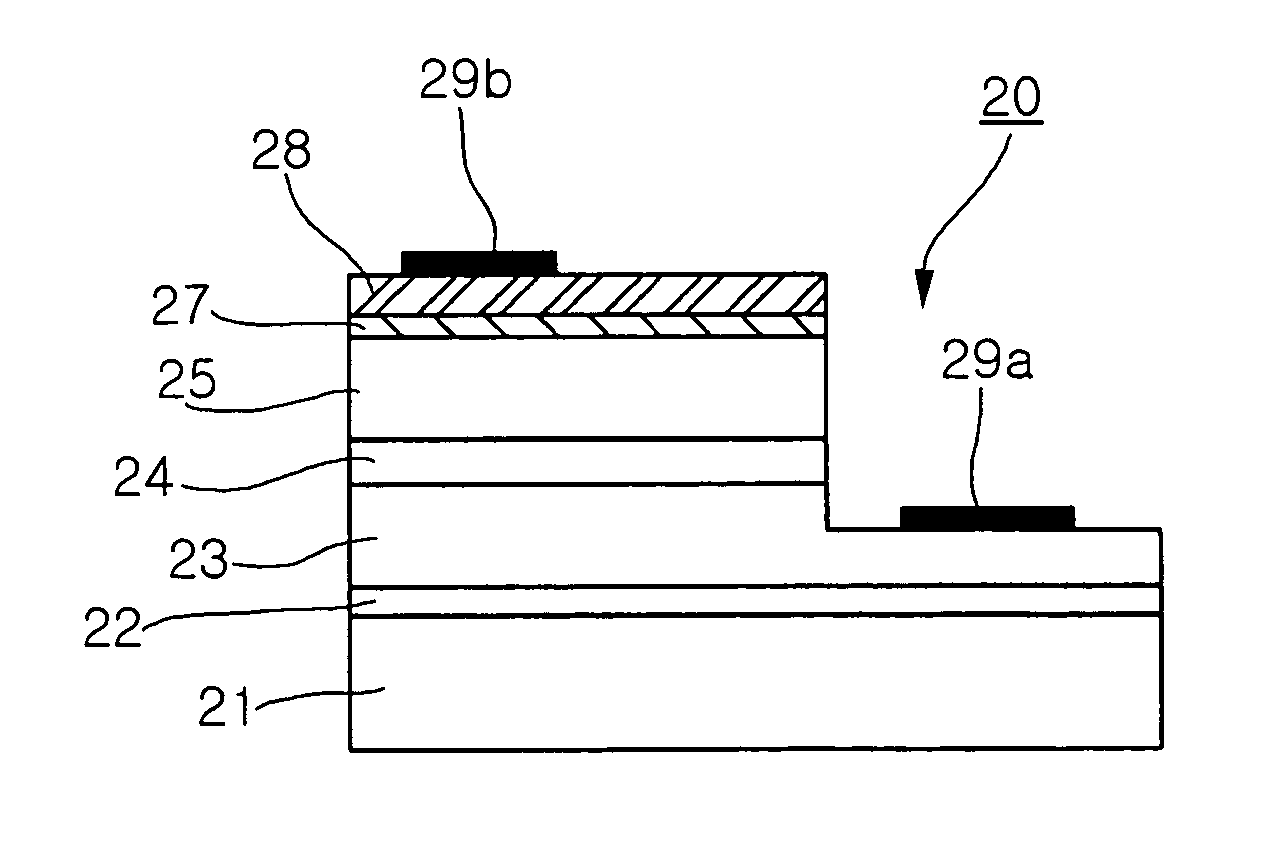
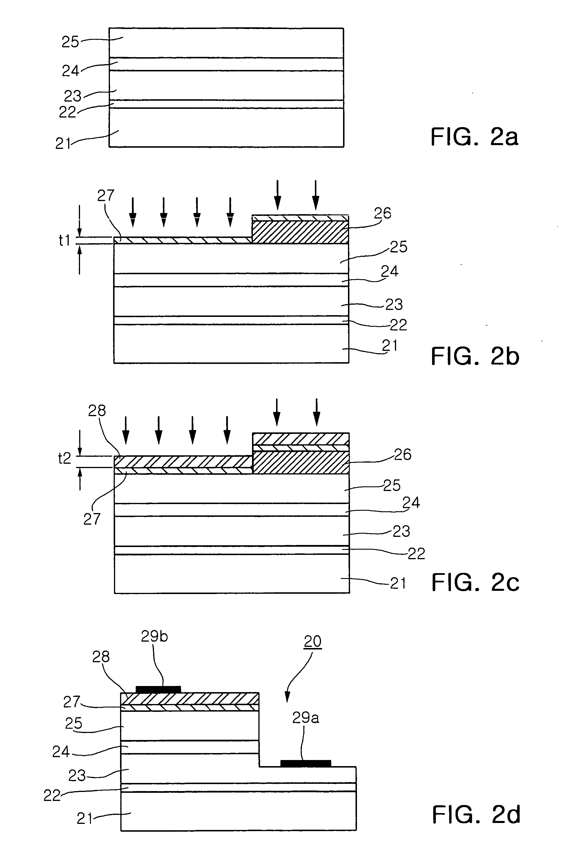
[0026]FIGS. 2a to 2d are sectional views illustrating a method of manufacturing a nitride semiconductor light emitting diode according to the invention.

[0027] The manufacturing method according to the invention, as shown in FIG. 2a, starts with forming an n-type nitride semiconductor layer 23, an active layer 24 and a p-type nitride semiconductor layer 25 sequentially on a substrate 21. The substrate 21 may be a sapphire substrate, a heterogeneous substrate made of e.g, SiC, or a homogenous substrate made of GaN. The substrate 21 may additionally include a buffer layer 22 made of e.g, AlN, GaN, or AlGaN grown at a low temperature. The nitride semiconductor layer (22,23,24 and 25) may be grown by metal-organic chemical vapor deposition (MOCVD), hydride vapor physe epitaxy (HVPE), and molecular beam epitaxy (MBE).

[0028] Thereafter, a photoresist is appli...


PUM


Abstract

The invention relates to a method of manufacturing a semiconductor light emitting diode. In the method, an n-type nitride semiconductor layer, an active layer and a p-type nitride semiconductor layer are formed sequentially on a substrate. Then, a nickel oxide (NiOx) film is directly deposited on the p-type semiconductor layer via reactive sputtering or reactive deposition in an oxidizing atmosphere. Also, a light transmissible conductive oxide layer is formed on the nickel oxide film.

Description

CLAIM OF PRIORITY [0001] This application claims the benefit of Korean Patent Application No. 2005-0031595 filed on Apr. 15, 2005 in the Korean Intellectual Property Office, the disclosure of which is incorporated herein by reference. BACKGROUND OF THE INVENTION [0002] 1. Field of the Invention [0003] The present invention relates to a method of manufacturing a nitride semiconductor light emitting diode. More particularly, the present invention relates to a novel method of manufacturing a nitride semiconductor light emitting diode which does not require heat processing to improve transmissibility of electrodes. [0004] 2. Description of the Related Art [0005] In general, a group III-nitride semiconductor is made of a material having a relatively high energy band gap (e.g., about 3.4 eV for a GaN semiconductor) and well-utilized for optical devices to generate short wavelength light such as blue or green light. The nitride semiconductor is chiefly made of a material having a compositi...

Claims


Application Information

Patent Timeline
IPC IPC(8): H01L21/00
CPCH01L33/32H01L33/42H01L33/40
Inventor RYU, YUNG HOKANG, PIL GEUN
Owner SAMSUNG ELECTRO MECHANICS CO LTD
Why Eureka
Try Eureka