Alumina layer with controlled texture
a technology of alumina layer and controlled texture, which is applied in the field of coating cutting tool inserts, can solve the problems of coating flaking, -al/sub>2/sub>o/sub>3 phase is more difficult to be nucleated and grown at reasonable cvd temperatures, and none of these systems have been commercially successful, so as to improve cutting properties, reduce dislocation density, and increase toughness
- Summary
- Abstract
- Description
- Claims
- Application Information
AI Technical Summary
Benefits of technology
Problems solved by technology
Method used
Image
Examples
example 1
[0054] Cemented carbide cutting inserts with a composition of 5.9% Co and balance WC (hardness about 1600 HV) were coated with a layer of MTCVD Ti(C,N). The thickness of the MTCVD layer was about 2 μm. On to this layer two different layers consisting of about 10 μm α-Al2O3 were deposited:
[0055] Layer a) contained a (104) textured layer and was deposited according to the present invention at 1000° C. The detailed process data is given in Table 1.
[0056] Layer b) was deposited according to the prior art.
[0057] Layer c) contained a (104) textured layer and was deposited according to the present invention at 800° C. The detailed process data is given in Table 2.
TABLE 1Deposition process for a Layer a) with (104) texture at 1000° C.:Step 1: Bonding layerGas mixtureTiCl4 = 2.8%AlCl3 = 0.8-4.2%CO = 5.8%CO2 = 2.2%N2 = 5-6%Balance: H2Duration60 minTemperature1000° C.Pressure100 mbarStep 2: PurgeGasAr = 100%Duration5 minTemperature1000 C.Pressure50 mbarStep 3: Pulse 1Gas mixtureTiCl4 = 1....
example 2
[0059] Layers a, b and c were studied using X-ray diffraction. The texture coefficients were determined are presented in Table 3. As clear from Table 3 the layer according to the present invention exhibits a strong (104) texture when deposited either at 1000° C. or 780° C. Typically, for this growth mode the (116) reflection is somewhat more profound than the other background reflections.
TABLE 3HklInvention, layer aPrior art, layer b,Invention, layer c0120.240.970.491044.301.143.131100.060.950.491130.190.990.410240.270.860.491160.941.090.99
example 3
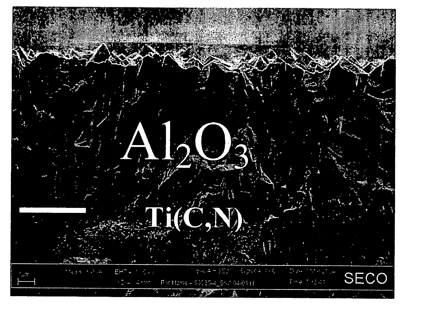
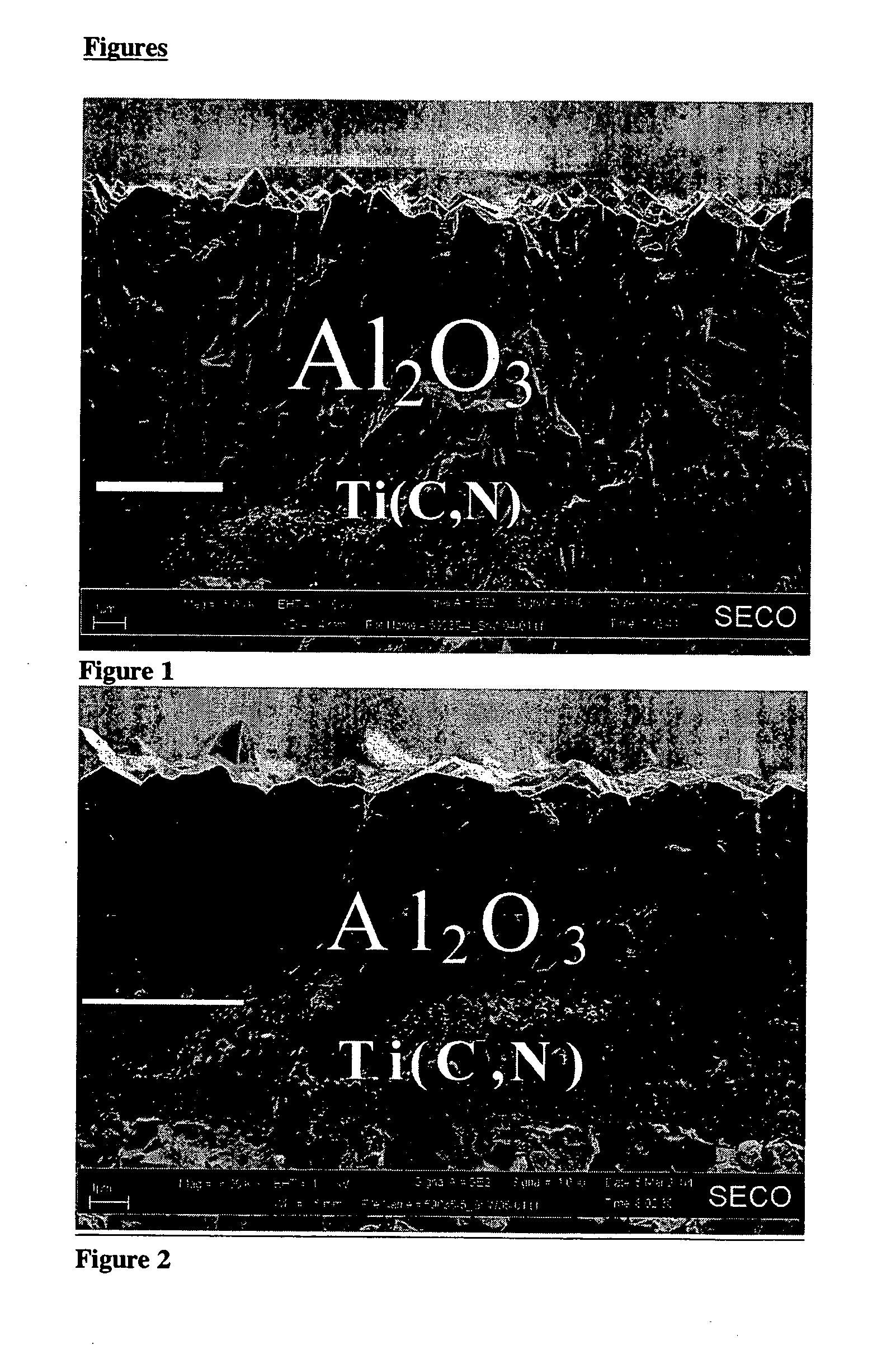
[0060] Layers a) and b) were studied using Scanning Electron Microscopy. The cross section images of the layers are shown in FIGS. 1 and 2, respectively. The differences in microstructure and morphology are clear.
PUM
| Property | Measurement | Unit |
|---|---|---|
| thickness | aaaaa | aaaaa |
| thickness | aaaaa | aaaaa |
| thickness | aaaaa | aaaaa |
Abstract
Description
Claims
Application Information
 - R&D
- Intellectual Property
- Life Sciences
- Materials
- Tech Scout
- Unparalleled Data Quality
- Higher Quality Content
- 60% Fewer Hallucinations
Browse by: Latest US Patents, China's latest patents, Technical Efficacy Thesaurus, Application Domain, Technology Topic, Popular Technical Reports.
© 2025 PatSnap. All rights reserved.Legal|Privacy policy|Modern Slavery Act Transparency Statement|Sitemap|About US| Contact US: help@patsnap.com


