
Material for forming fine pattern and method for forming fine pattern using the same

a technology of fine pattern and fine pattern, which is applied in the field of fine pattern forming materials, can solve the problems of difficult formation of fine resist patterns over the limit of wavelength, high cost of light-exposure devices for short wavelength and devices using phase-shift masks, and a large etc., to achieve the effect of reducing the number of development defects, reducing the amount of coating, and high accuracy

Inactive Publication Date: 2006-08-17
MERCK PATENT GMBH
View PDF19 Cites 20 Cited by
  • Summary
  • Abstract
  • Description
  • Claims
  • Application Information

AI Technical Summary

Benefits of technology

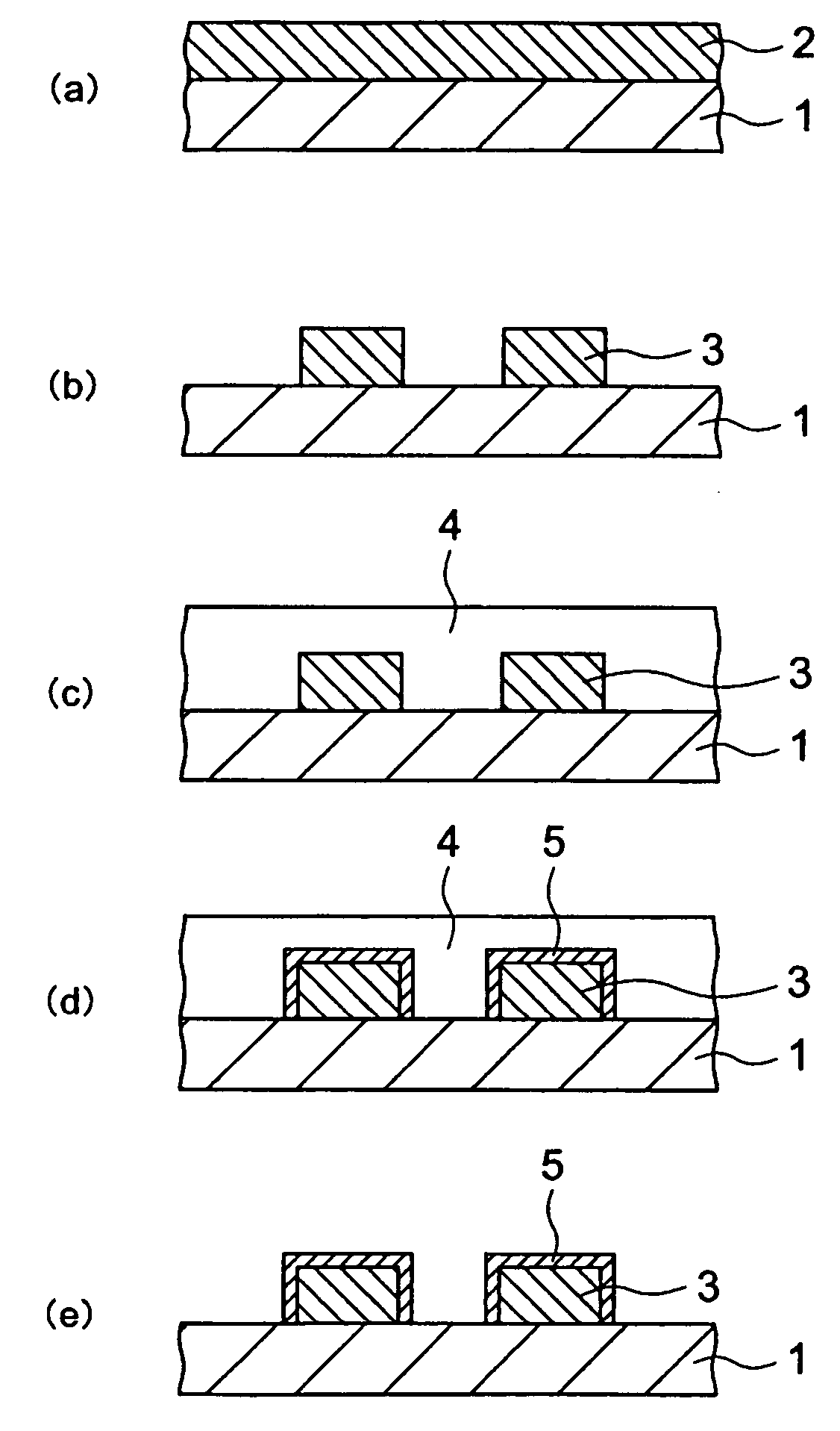
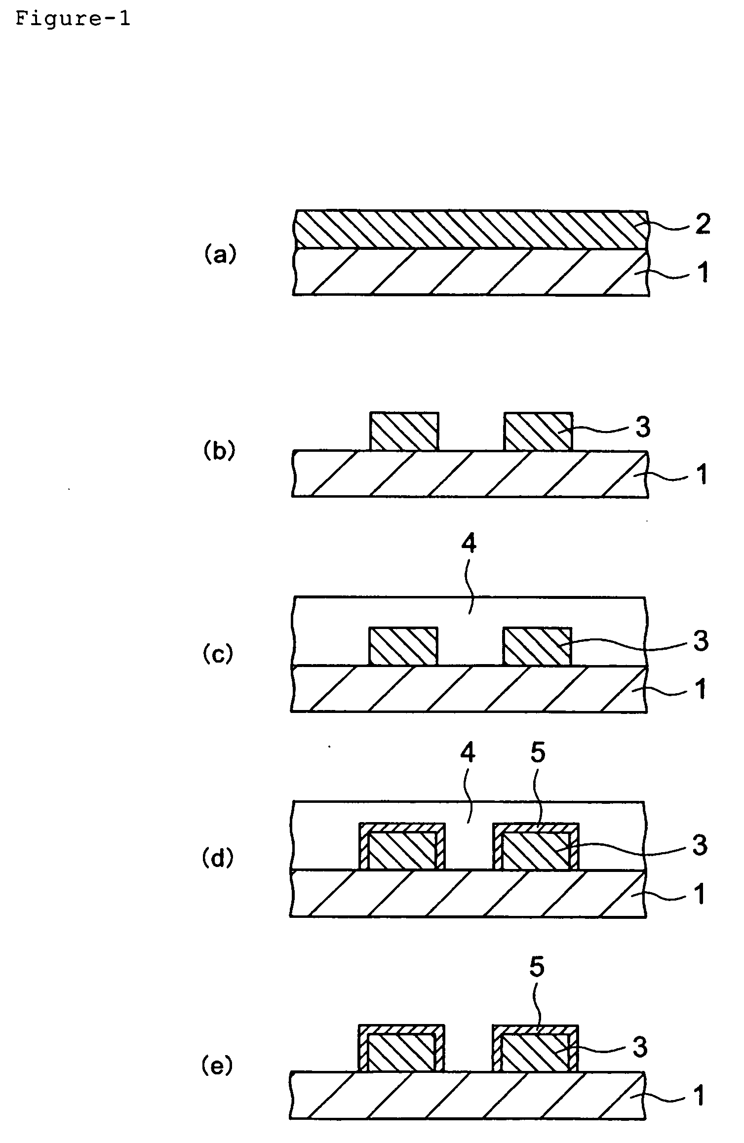
[0014] In the present invention, a water-soluble fine pattern forming material can be obtained by incorporating an amine compound into the fine pattern forming material. By using this water-soluble fine pattern forming material, a coated layer is formed on a resist pattern generating an acid by heating, etc., the coated layer in the vicinity of the resist pattern is crosslinked or cured by heating, is developed and the number of development defects are also reduced by water development to be able to form a pattern without problems in a practical use. And also by further incorporating a surfactant into the fine pattern forming material, the fine pattern forming material wherein a minimum coating amount is reduced and a pattern forming method using the same can be offered. By the fine pattern forming material of the present invention and the fine pattern forming method applying this fine pattern forming material, in a fine processing for manufacturing electronic parts such as a semiconductor, etc. or a three-dimensional fine structured article, a pattern having a size of a limit resolution of an exposure to light or less can be formed in accordance with a design rule as designed in high accuracy, high-through-put and inexpensively.

Problems solved by technology

In the conventional photolithographic technology using light exposure, however, a formation of fine resist patterns exceeding the limit of wavelength is difficult and the light-exposure devices for short wavelength and the devices using a phase-shift mask are expensive.
This is because of incomplete removal of uncrosslinked area of the coated layer by a development only with water due to poor solubility of a fine pattern forming material so far known in water, generating a residue of dissolution to cause a lot of development defects.
Because of this, a fine pattern formation by a development only by water is difficult from the view point of development defects at present.

Method used


Image

  • Material for forming fine pattern and method for forming fine pattern using the same
  • Material for forming fine pattern and method for forming fine pattern using the same
  • Material for forming fine pattern and method for forming fine pattern using the same

Examples


example-1

(Preparation of Fine Pattern Forming Material)

[0037] 100 parts by weight of polyvinyl acetal (acetylization degree: 12 mol %, acetalization degree: 30 mol %), 20 parts by weight of a water-soluble crosslinking agent of a urea derivative (methoxymethyl imidazolidinone) and 4 parts by weight of tetramethylammonium hydroxide (TMAH) were solved in 1470 parts by weight of a mixed solvent of pure water and isopropyl alcohol which is a water-soluble organic solvent (5 parts by weight of isopropyl alcohol relative to 95 parts by weight of pure water), to prepare the fine pattern forming material A (Composition A). The pH value thereof was 8.8. Next, Composition A was put into the following “Inspection for a film thickness of a coated layer” and “Inspection for development defects”.

(Inspection for a Film Thickness of a Coated Layer)

[0038] AZ KrF-17B 80 (manufactured by Clariant Co. AZ is a registered trademark, the followings are the same.) was spin-coated on a 6-inch bare silicon wafer...

example-2

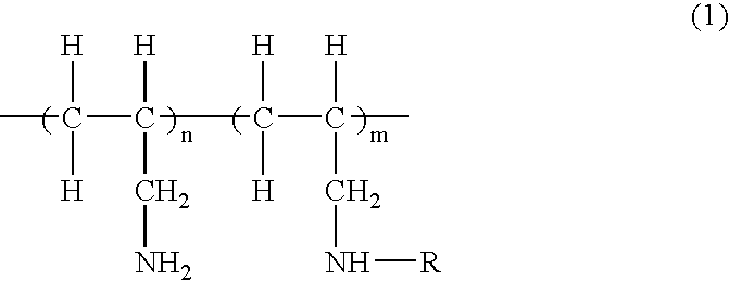
[0040] Except using partially methoxy carbonylated polyallylamine (PAA) represented by the general formula (2) below (n=50, m=50, average molecular weight: 3000) in place of TMAH, the same manner was carried out as Example-1 to prepare a fine pattern forming material B (Composition B). The pH value thereof was 7.3. “Inspection for a film thickness of a coated layer” and “Inspection for development defects” were carried out in the same manner as Example-1. The result is shown in Table 1.

example-3

[0041] Except using partially methoxy carbonylated polyallylamine represented by the general formula (2) above (n=50, m=50, average molecular weight: 5000) in place of TMAH, the same manner was carried out as Example-1 to prepare a fine pattern forming material C (Composition C). The pH value thereof was 7.3. “Inspection for a film thickness of a coated layer” and “Inspection for development defects” were carried out in the same manner as Example-1. The result is shown in Table 1. Composition C was put into the following “Evaluation for coatability”.

(Evaluation for Coatability)

[0042] Composition C was output on an 8-inch bare silicon wafer by 5, 7.5 and 10 cc, spin-coated at 3500 rpm and baking on a direct hotplate at 85° C. for 70 seconds to form a film of a radiation sensitive resin composition for forming a fine pattern. At this time minimum output volume was gained by observing whether or not the coating reached to an edge of the wafer evenly. The result is shown in Table-2. ...


PUM


Abstract

In the method wherein a resist pattern is miniaturized effectively by applying a fine pattern forming material, the fine pattern forming material used for providing with a cured coated layer pattern, wherein development defects are reduced by water development is offered, wherein the fine pattern forming material comprises a water-soluble resin, a water-soluble crosslinking agent and water or a mixed solution consisting of water and a water-soluble organic solvent, and further comprises an amine compound.

Description

TECHNICAL FIELD [0001] The present invention relates to a fine pattern forming material, wherein a development by water comes to be possible without using a developer for an exclusive use by reducing a separation size between a resist pattern and a resist pattern or a pattern hole aperture size which is already formed upon forming a resist pattern in a semiconductor process as well as a finer pattern can be formed, and to a pattern forming method using the fine pattern forming material. BACKGROUND ART [0002] In various fields including manufacturing a semiconductor device such as LSI, forming a liquid crystal display face such as LCD panels, and manufacturing circuit substrates for a thermal head and so on, a formation of resist patterns on substrates is conducted for a formation of fine elements or for fine processing. Formation of these resist patterns employs a so-called photolithographic method which involves a light exposure of a photosensitive resin composition by a selective ...

Claims


Application Information

Patent Timeline
IPC IPC(8): C12M1/34G03F7/40
CPCG03F7/40G03F7/11
Inventor TAKAHASHI, KIYOHISATAKANO, YUSUKE
Owner MERCK PATENT GMBH
Learn More